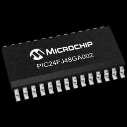
MCU 16-bit PIC24 PIC RISC 48KB Flash 2.5V/3.3V 28-Pin SOIC W Tube, PIC24FJ48GA002-E/SO, Microchip

This family introduces a new line of Microchip devices: a 16-bit microcontroller family with a broad peripheral feature set and enhanced computational performance. The PIC24FJ64GA004 family offers a new migration option for those high-performance applications which may be outgrowing their 8-bit platforms, but don’t require the numerical processing power of a digital signal processor. Core Features 16-BIT ARCHITECTURE Central to all PIC24F devices is the 16-bit modified Harvard architecture, first introduced with Microchip’s dsPIC digital signal controllers. The PIC24F CPU core offers a wide range of enhancements, such as: 16-bit data and 24-bit address paths with the ability to move information between data and memory spaces Linear addressing of up to 12 Mbytes (program space) and 64 Kbytes (data) A 16-element working register array with built-in software stack support A 17 x 17 hardware multiplier with support for integer math Hardware support for 32 by 16-bit division An instruction set that supports multiple addressing modes and is optimized for high-level languages such as ‘C’ Operational performance up to 16 MIPS POWER-SAVING TECHNOLOGY All of the devices in the PIC24FJ64GA004 family incorporate a range of features that can significantly reduce power consumption during operation. Key items include: On-the-Fly Clock Switching: The device clock can be changed under software control to the Timer1 source or the internal, low-power RC oscillator during operation, allowing the user to incorporate power-saving ideas into their software designs. Doze Mode Operation: When timing-sensitive applications, such as serial communications, require the uninterrupted operation of peripherals, the CPU clock speed can be selectively reduced, allowing incremental power savings without missing a beat. Instruction-Based Power-Saving Modes: The microcontroller can suspend all operations, or selectively shut down its core while leaving its peripherals active, with a single instruction in software. OSCILLATOR OPTIONS AND FEATURES All of the devices in the PIC24FJ64GA004 family offer five different oscillator options, allowing users a range of choices in developing application hardware. These include: Two Crystal modes using crystals or ceramic resonators. Two External Clock modes offering the option of a divide-by-2 clock output. A Fast Internal Oscillator (FRC) with a nominal 8 MHz output, which can also be divided under software control to provide clock speeds as low as 31 kHz. A Phase Lock Loop (PLL) frequency multiplier, available to the External Oscillator modes and the FRC oscillator, which allows clock speeds of up to 32 MHz. A separate internal RC oscillator (LPRC) with a fixed 31 kHz output, which provides a low-power option for timing-insensitive applications. The internal oscillator block also provides a stable reference source for the Fail-Safe Clock Monitor. This option constantly monitors the main clock source against a reference signal provided by the internal oscillator and enables the controller to switch to the internal oscillator, allowing for continued low-speed operation or a safe application shutdown. EASY MIGRATION Regardless of the memory size, all devices share the same rich set of peripherals, allowing for a smooth migration path as applications grow and evolve. The consistent pinout scheme used throughout the entire family also aids in migrating to the next larger device. This is true when moving between devices with the same pin count, or even jumping from 28-pin to 44-pin devices.

  • High-Performance CPU:
  • Modified Harvard Architecture
  • Up to 16 MIPS Operation @ 32 MHz
  • 8 MHz Internal Oscillator with 4x PLL Option and Multiple Divide Options
  • 17-Bit by 17-Bit Single-Cycle Hardware Multiplier
  • 32-Bit by 16-Bit Hardware Divider
  • 16-Bit x 16-Bit Working Register Array
  • C Compiler Optimized Instruction Set Architecture:
    • 76 base instructions
    • Flexible addressing modes
  • Two Address Generation Units for Separate Read and Write Addressing of Data Memory
  • Special Microcontroller Features:
  • Operating Voltage Range of 2.0V to 3.6V
  • 5.5V Tolerant Input (digital pins only)
  • High-Current Sink/Source (18 mA/18 mA) on All I/O Pins
  • Flash Program Memory:
    • 10,000 erase/write
    • 20-year data retention minimum
  • Power Management modes:
    • Sleep, Idle, Doze and Alternate Clock modes
    • Operating current 650 µA/MIPS typical at 2.0V
    • Sleep current 150 nA typical at 2.0V
  • Fail-Safe Clock Monitor Operation:
    • Detects clock failure and switches to on-chip, low-power RC oscillator
  • On-Chip, 2.5V Regulator with Tracking mode
  • Power-on Reset (POR), Power-up Timer (PWRT) and Oscillator Start-up Timer (OST)
  • Flexible Watchdog Timer (WDT) with On-Chip, Low-Power RC Oscillator for Reliable Operation
  • In-Circuit Serial Programming™ (ICSP™) and In-Circuit Debug (ICD) via 2 Pins
  • JTAG Boundary Scan Support
  • Analog Features:
  • 10-Bit, up to 13-Channel Analog-to-Digital Converter:
    • 500 ksps conversion rate
    • Conversion available during Sleep and Idle
  • Dual Analog Comparators with Programmable Input/Output Configuration
  • Peripheral Features:
  • Peripheral Pin Select:
    • Allows independent I/O mapping of many peripherals
    • Up to 26 available pins (44-pin devices)
    • Continuous hardware integrity checking and safety interlocks prevent unintentional configuration changes
  • 8-Bit Parallel Master/Slave Port (PMP/PSP):
    • Up to 16-bit multiplexed addressing, with up to 11 dedicated address pins on 44-pin devices
    • Programmable polarity on control lines
  • Hardware Real-Time Clock/Calendar (RTCC):
    • Provides clock, calendar and alarm functions
  • Programmable Cyclic Redundancy Check (CRC)
  • Two 3-Wire/4-Wire SPI modules (support 4 Frame modes) with 8-Level FIFO Buffer
  • Two I2C™ modules support Multi-Master/Slave mode and 7-Bit/10-Bit Addressing
  • Two UART modules:
    • Supports RS-485, RS-232, and LIN 1.2
    • On-chip hardware encoder/decoder for IrDA®
    • Auto-wake-up on Start bit
    • Auto-Baud Detect
    • 4-level deep FIFO buffer
  • Five 16-Bit Timers/Counters with Programmable Prescaler
  • Five 16-Bit Capture Inputs
  • Five 16-Bit Compare/PWM Outputs
  • Configurable Open-Drain Outputs on Digital I/O Pins
  • Up to 4 External Interrupt Sources
Характеристики

Schedule_b

8542310000

Бренд

Operating_temperature

-40 to 125 °C

Pin_count

28

Product_dimensions

17.87 x 7.49 x 2.31 mm

Program_memory_size

48 KB

Ram_size

8 KB

Screening_level

Extended

On_chip_adc

10-chx10-bit

Specifications

https://4donline.ihs.com/images/VipMasterIC/IC/MCHP/MCHPS05315/MCHPS05315-1.pdf?hkey=52A5661711E402568146F3353EA87419

Supplier_package

SOIC W

Watchdog

1

Max_speed

32 MHz

Number_of_timers

5

Operating_supply_voltage

2.5, 3.3 V

Country_of_origin

China

Instruction_set_architecture

RISC

Data_bus_width

16 Bit

Device_core

PIC

Eccn

3A991.A.2

Htsn

8542310001

Тип интерфейса

I2C/SPI/UART

Number_of_programmable_i_os

21

Lead_finish

Matte Tin

Max_expanded_memory_size

12 MB

Max_operating_supply_voltage

2.75, 3.6 V

Max_processing_temp

260 °C

Min_operating_supply_voltage

2, 2.2 V

Mounting

Surface Mount

Msl_level

1, 3

Артикул: PIC24FJ48GA002-E/SO

Описание

This family introduces a new line of Microchip devices: a 16-bit microcontroller family with a broad peripheral feature set and enhanced computational performance. The PIC24FJ64GA004 family offers a new migration option for those high-performance applications which may be outgrowing their 8-bit platforms, but don’t require the numerical processing power of a digital signal processor. Core Features 16-BIT ARCHITECTURE Central to all PIC24F devices is the 16-bit modified Harvard architecture, first introduced with Microchip’s dsPIC digital signal controllers. The PIC24F CPU core offers a wide range of enhancements, such as: 16-bit data and 24-bit address paths with the ability to move information between data and memory spaces Linear addressing of up to 12 Mbytes (program space) and 64 Kbytes (data) A 16-element working register array with built-in software stack support A 17 x 17 hardware multiplier with support for integer math Hardware support for 32 by 16-bit division An instruction set that supports multiple addressing modes and is optimized for high-level languages such as ‘C’ Operational performance up to 16 MIPS POWER-SAVING TECHNOLOGY All of the devices in the PIC24FJ64GA004 family incorporate a range of features that can significantly reduce power consumption during operation. Key items include: On-the-Fly Clock Switching: The device clock can be changed under software control to the Timer1 source or the internal, low-power RC oscillator during operation, allowing the user to incorporate power-saving ideas into their software designs. Doze Mode Operation: When timing-sensitive applications, such as serial communications, require the uninterrupted operation of peripherals, the CPU clock speed can be selectively reduced, allowing incremental power savings without missing a beat. Instruction-Based Power-Saving Modes: The microcontroller can suspend all operations, or selectively shut down its core while leaving its peripherals active, with a single instruction in software. OSCILLATOR OPTIONS AND FEATURES All of the devices in the PIC24FJ64GA004 family offer five different oscillator options, allowing users a range of choices in developing application hardware. These include: Two Crystal modes using crystals or ceramic resonators. Two External Clock modes offering the option of a divide-by-2 clock output. A Fast Internal Oscillator (FRC) with a nominal 8 MHz output, which can also be divided under software control to provide clock speeds as low as 31 kHz. A Phase Lock Loop (PLL) frequency multiplier, available to the External Oscillator modes and the FRC oscillator, which allows clock speeds of up to 32 MHz. A separate internal RC oscillator (LPRC) with a fixed 31 kHz output, which provides a low-power option for timing-insensitive applications. The internal oscillator block also provides a stable reference source for the Fail-Safe Clock Monitor. This option constantly monitors the main clock source against a reference signal provided by the internal oscillator and enables the controller to switch to the internal oscillator, allowing for continued low-speed operation or a safe application shutdown. EASY MIGRATION Regardless of the memory size, all devices share the same rich set of peripherals, allowing for a smooth migration path as applications grow and evolve. The consistent pinout scheme used throughout the entire family also aids in migrating to the next larger device. This is true when moving between devices with the same pin count, or even jumping from 28-pin to 44-pin devices.

  • High-Performance CPU:
  • Modified Harvard Architecture
  • Up to 16 MIPS Operation @ 32 MHz
  • 8 MHz Internal Oscillator with 4x PLL Option and Multiple Divide Options
  • 17-Bit by 17-Bit Single-Cycle Hardware Multiplier
  • 32-Bit by 16-Bit Hardware Divider
  • 16-Bit x 16-Bit Working Register Array
  • C Compiler Optimized Instruction Set Architecture:
    • 76 base instructions
    • Flexible addressing modes
  • Two Address Generation Units for Separate Read and Write Addressing of Data Memory
  • Special Microcontroller Features:
  • Operating Voltage Range of 2.0V to 3.6V
  • 5.5V Tolerant Input (digital pins only)
  • High-Current Sink/Source (18 mA/18 mA) on All I/O Pins
  • Flash Program Memory:
    • 10,000 erase/write
    • 20-year data retention minimum
  • Power Management modes:
    • Sleep, Idle, Doze and Alternate Clock modes
    • Operating current 650 µA/MIPS typical at 2.0V
    • Sleep current 150 nA typical at 2.0V
  • Fail-Safe Clock Monitor Operation:
    • Detects clock failure and switches to on-chip, low-power RC oscillator
  • On-Chip, 2.5V Regulator with Tracking mode
  • Power-on Reset (POR), Power-up Timer (PWRT) and Oscillator Start-up Timer (OST)
  • Flexible Watchdog Timer (WDT) with On-Chip, Low-Power RC Oscillator for Reliable Operation
  • In-Circuit Serial Programming™ (ICSP™) and In-Circuit Debug (ICD) via 2 Pins
  • JTAG Boundary Scan Support
  • Analog Features:
  • 10-Bit, up to 13-Channel Analog-to-Digital Converter:
    • 500 ksps conversion rate
    • Conversion available during Sleep and Idle
  • Dual Analog Comparators with Programmable Input/Output Configuration
  • Peripheral Features:
  • Peripheral Pin Select:
    • Allows independent I/O mapping of many peripherals
    • Up to 26 available pins (44-pin devices)
    • Continuous hardware integrity checking and safety interlocks prevent unintentional configuration changes
  • 8-Bit Parallel Master/Slave Port (PMP/PSP):
    • Up to 16-bit multiplexed addressing, with up to 11 dedicated address pins on 44-pin devices
    • Programmable polarity on control lines
  • Hardware Real-Time Clock/Calendar (RTCC):
    • Provides clock, calendar and alarm functions
  • Programmable Cyclic Redundancy Check (CRC)
  • Two 3-Wire/4-Wire SPI modules (support 4 Frame modes) with 8-Level FIFO Buffer
  • Two I2C™ modules support Multi-Master/Slave mode and 7-Bit/10-Bit Addressing
  • Two UART modules:
    • Supports RS-485, RS-232, and LIN 1.2
    • On-chip hardware encoder/decoder for IrDA®
    • Auto-wake-up on Start bit
    • Auto-Baud Detect
    • 4-level deep FIFO buffer
  • Five 16-Bit Timers/Counters with Programmable Prescaler
  • Five 16-Bit Capture Inputs
  • Five 16-Bit Compare/PWM Outputs
  • Configurable Open-Drain Outputs on Digital I/O Pins
  • Up to 4 External Interrupt Sources

Детали

Schedule_b

8542310000

Бренд

Operating_temperature

-40 to 125 °C

Pin_count

28

Product_dimensions

17.87 x 7.49 x 2.31 mm

Program_memory_size

48 KB

Ram_size

8 KB

Screening_level

Extended

On_chip_adc

10-chx10-bit

Specifications

https://4donline.ihs.com/images/VipMasterIC/IC/MCHP/MCHPS05315/MCHPS05315-1.pdf?hkey=52A5661711E402568146F3353EA87419

Supplier_package

SOIC W

Watchdog

1

Max_speed

32 MHz

Number_of_timers

5

Operating_supply_voltage

2.5, 3.3 V

Country_of_origin

China

Instruction_set_architecture

RISC

Data_bus_width

16 Bit

Device_core

PIC

Eccn

3A991.A.2

Htsn

8542310001

Тип интерфейса

I2C/SPI/UART

Number_of_programmable_i_os

21

Lead_finish

Matte Tin

Max_expanded_memory_size

12 MB

Max_operating_supply_voltage

2.75, 3.6 V

Max_processing_temp

260 °C

Min_operating_supply_voltage

2, 2.2 V

Mounting

Surface Mount

Msl_level

1, 3