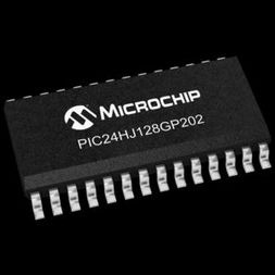
MCU 16-bit PIC24 PIC RISC 128KB Flash 3.3V 28-Pin SOIC W Tube, PIC24HJ128GP202-I/SO, Microchip

PIC24HJ32GP304 is High-Performance, 16-bit Microcontrollers The PIC24HJ32GP304 CPU modules have a 16-bit (data) modified Harvard architecture with an enhanced instruction set and addressing modes. The CPU has a 24-bit instruction word with a variable length opcode field. The Program Counter (PC) is 23 bits wide and addresses up to 4M x 24 bits of user program memory space. The actual amount of program memory implemented varies by device. A single-cycl e instruction prefetch mechanism is used to help maintain throughput and provides predictable execution. Overhead-free, single-cycle program loop constructs are supported using the REPEAT instruction, which is interruptible at any time The PIC24HJ32GP304 devices have sixteen, 16-bit working registers in the programmer’s model. Each of the working registers can serve as a data, address or address offset register. The 16th working register (W15) op erates as a software Stack Pointer (SP) for interrupts and calls The instruction set includes many addressing modes and is designed for optimum C compiler efficiency. For most instructions, the devices are capable of executing a data (or program data) memory read, a working register (data) read, a data memory write and a program (instruction) memory read per instruction cycle. As a result, three pa rameter instructions can be supported, allowing A + B = C operations to be executed in a single cycleThe data space can be linearly addressed as 32K words or 64 Kbytes using an Addr ess Generation Unit (AGU). The upper 32 Kbytes of the data space memory map can optionally be mapped into program space at any 16K pro- gram word boundary defined by the 8-bit Program Space Visibility Page register (P SVPAG). The program to data space mapping feature lets any instruction access pro- gram space as if it were data space. The data space also includes 2 Kbytes of DMA RAM, which is primarily used for DMA data transfers, but this may be used as general purpose RAMThe PIC24HJ32GP304 devices feature a 17-bit by 17-bit, single-cycle multiplier. The multiplier can perform signed, unsigned and mixed-sign multiplication. Using a 17-bit by 17-bit multiplier for 16-bit by 16-bit multiplication makes mixed-sign multiplication possible The PIC24HJ32GP304 devices support 16/16 and 32/16 integer divide operations. All divide in structions are iterative operations. They must be executed within a REPEAT loop, resulting in a total execution time of 19 instruction cycles. The divide operation can be interru pted during any of those 19 cycles without loss of data A multi-bit data shifter is used to perform up to a 16-bit, left or right shift in a single cycle.

  • Operating Range:
  • Up to 40 MIPS operation (at 3.0-3.6V):
    • Industrial temperature range (-40°C to +85°C)
    • Extended temperature range (-40°C to +125°C)
  • Up to 20 MIPS operation (at 3.0-3.6V):
    • High temperature range (-40°C to +150°C)
  • High-Performance CPU:
  • Modified Harvard architecture
  • C compiler optimized instruction set
  • 16-bit wide data path
  • 24-bit wide instructions
  • Linear program memory addressing up to 4M instruction words
  • Linear data memory addressing up to 64 Kbytes
  • 71 base instructions: mostly 1 word/1 cycle
  • Flexible and powerful addressing modes
  • 16 x 16 multiply operations
  • 32/16 and 16/16 divide operations
  • Up to ±16-bit shifts for up to 40-bit data
  • Direct Memory Access (DMA):
  • 8-channel hardware DMA
  • Up to 2 Kbytes dual ported DMA buffer area (DMA RAM) to store data transferred via DMA:
    • Allows data transfer between RAM and a peripheral while CPU is executing code (no cycle stealing)
  • Most peripherals support DMA
  • On-Chip Flash and SRAM:
  • Flash program memory (up to 128 Kbytes)
  • Data SRAM (up to 8 Kbytes)
  • Boot, Secure and General Security for program Flash
  • Timers/Capture/Compare/PWM:
  • Timer/Counters, up to five 16-bit timers:
    • Can pair up to make two 32-bit timers
    • One timer runs as a Real-Time Clock with an external 32.768 kHz oscillator
    • Programmable prescaler
  • Input Capture (up to four channels):
    • Capture on up, down or both edges
    • 16-bit capture input functions
    • 4-deep FIFO on each capture
  • Output Compare (up to four channels):
    • Single or Dual 16-bit Compare mode
    • 16-bit Glitchless PWM mode
  • Hardware Real-Time Clock and Calendar (RTCC):
    • Provides clock, calendar and alarm functions
  • Interrupt Controller:
  • 5-cycle latency
  • Up to 45 available interrupt sources
  • Up to three external interrupts
  • Seven programmable priority levels
  • Five processor exceptions
  • Digital I/O:
  • Peripheral pin Select functionality
  • Up to 35 programmable digital I/O pins
  • Wake-up/Interrupt-on-Change for up to 31 pins
  • Output pins can drive from 3.0V to 3.6V
  • Up to 5.5V output with open drain configuration on 5V tolerant pins with external pull-up
  • 4 mA sink on all I/O pins
  • Communication Modules:
  • 4-wire SPI (up to two modules):
    • Framing supports I/O interface to simple codecs
    • Supports 8-bit and 16-bit data
    • Supports all serial clock formats and sampling modes
  • I2C:
    • Full Multi-Master Slave mode support
    • 7-bit and 10-bit addressing
    • Bus collision detection and arbitration
    • Integrated signal conditioning
    • Slave address masking
  • UART (up to two modules):
    • Interrupt on address bit detect
    • Interrupt on UART error
    • Wake-up on Start bit from Sleep mode
    • 4-character TX and RX FIFO buffers
    • LIN 2.0 bus support
    • IrDA encoding and decoding in hardware
    • High-Speed Baud mode
    • Hardware Flow Control with CTS and RTS
  • Enhanced CAN (ECAN™ module) 2.0B active:
    • Up to eight transmit and up to 32 receive buffers
    • 16 receive filters and three masks
    • Loopback, Listen Only and Listen All
    • Messages modes for diagnostics and bus monitoring
    • Wake-up on CAN message

Характеристики

Schedule_b

8542310000

Бренд

Operating_temperature

-40 to 85 °C

Pin_count

28

Product_dimensions

17.87 x 7.49 x 2.31 mm

Screening_level

Industrial

On_chip_adc

10-chx12-bit

Specifications

https://4donline.ihs.com/images/VipMasterIC/IC/MCHP/MCHPS03728/MCHPS03728-1.pdf?hkey=52A5661711E402568146F3353EA87419

Supplier_package

SOIC W

Watchdog

1

Max_speed

40 MHz

Number_of_timers

5

Operating_supply_voltage

3.3 V

Country_of_origin

China

Instruction_set_architecture

RISC

Data_bus_width

16 Bit

Device_core

PIC

Eccn

3A991.A.2

Htsn

8542310001

Тип интерфейса

I2C/SPI/UART

Number_of_programmable_i_os

21

Lead_finish

Matte Tin

Max_expanded_memory_size

12 MB

Max_processing_temp

260 °C

Mounting

Surface Mount

Msl_level

1, 3

Артикул: PIC24HJ128GP202-I/SO

Описание

PIC24HJ32GP304 is High-Performance, 16-bit Microcontrollers The PIC24HJ32GP304 CPU modules have a 16-bit (data) modified Harvard architecture with an enhanced instruction set and addressing modes. The CPU has a 24-bit instruction word with a variable length opcode field. The Program Counter (PC) is 23 bits wide and addresses up to 4M x 24 bits of user program memory space. The actual amount of program memory implemented varies by device. A single-cycl e instruction prefetch mechanism is used to help maintain throughput and provides predictable execution. Overhead-free, single-cycle program loop constructs are supported using the REPEAT instruction, which is interruptible at any time The PIC24HJ32GP304 devices have sixteen, 16-bit working registers in the programmer’s model. Each of the working registers can serve as a data, address or address offset register. The 16th working register (W15) op erates as a software Stack Pointer (SP) for interrupts and calls The instruction set includes many addressing modes and is designed for optimum C compiler efficiency. For most instructions, the devices are capable of executing a data (or program data) memory read, a working register (data) read, a data memory write and a program (instruction) memory read per instruction cycle. As a result, three pa rameter instructions can be supported, allowing A + B = C operations to be executed in a single cycleThe data space can be linearly addressed as 32K words or 64 Kbytes using an Addr ess Generation Unit (AGU). The upper 32 Kbytes of the data space memory map can optionally be mapped into program space at any 16K pro- gram word boundary defined by the 8-bit Program Space Visibility Page register (P SVPAG). The program to data space mapping feature lets any instruction access pro- gram space as if it were data space. The data space also includes 2 Kbytes of DMA RAM, which is primarily used for DMA data transfers, but this may be used as general purpose RAMThe PIC24HJ32GP304 devices feature a 17-bit by 17-bit, single-cycle multiplier. The multiplier can perform signed, unsigned and mixed-sign multiplication. Using a 17-bit by 17-bit multiplier for 16-bit by 16-bit multiplication makes mixed-sign multiplication possible The PIC24HJ32GP304 devices support 16/16 and 32/16 integer divide operations. All divide in structions are iterative operations. They must be executed within a REPEAT loop, resulting in a total execution time of 19 instruction cycles. The divide operation can be interru pted during any of those 19 cycles without loss of data A multi-bit data shifter is used to perform up to a 16-bit, left or right shift in a single cycle.

  • Operating Range:
  • Up to 40 MIPS operation (at 3.0-3.6V):
    • Industrial temperature range (-40°C to +85°C)
    • Extended temperature range (-40°C to +125°C)
  • Up to 20 MIPS operation (at 3.0-3.6V):
    • High temperature range (-40°C to +150°C)
  • High-Performance CPU:
  • Modified Harvard architecture
  • C compiler optimized instruction set
  • 16-bit wide data path
  • 24-bit wide instructions
  • Linear program memory addressing up to 4M instruction words
  • Linear data memory addressing up to 64 Kbytes
  • 71 base instructions: mostly 1 word/1 cycle
  • Flexible and powerful addressing modes
  • 16 x 16 multiply operations
  • 32/16 and 16/16 divide operations
  • Up to ±16-bit shifts for up to 40-bit data
  • Direct Memory Access (DMA):
  • 8-channel hardware DMA
  • Up to 2 Kbytes dual ported DMA buffer area (DMA RAM) to store data transferred via DMA:
    • Allows data transfer between RAM and a peripheral while CPU is executing code (no cycle stealing)
  • Most peripherals support DMA
  • On-Chip Flash and SRAM:
  • Flash program memory (up to 128 Kbytes)
  • Data SRAM (up to 8 Kbytes)
  • Boot, Secure and General Security for program Flash
  • Timers/Capture/Compare/PWM:
  • Timer/Counters, up to five 16-bit timers:
    • Can pair up to make two 32-bit timers
    • One timer runs as a Real-Time Clock with an external 32.768 kHz oscillator
    • Programmable prescaler
  • Input Capture (up to four channels):
    • Capture on up, down or both edges
    • 16-bit capture input functions
    • 4-deep FIFO on each capture
  • Output Compare (up to four channels):
    • Single or Dual 16-bit Compare mode
    • 16-bit Glitchless PWM mode
  • Hardware Real-Time Clock and Calendar (RTCC):
    • Provides clock, calendar and alarm functions
  • Interrupt Controller:
  • 5-cycle latency
  • Up to 45 available interrupt sources
  • Up to three external interrupts
  • Seven programmable priority levels
  • Five processor exceptions
  • Digital I/O:
  • Peripheral pin Select functionality
  • Up to 35 programmable digital I/O pins
  • Wake-up/Interrupt-on-Change for up to 31 pins
  • Output pins can drive from 3.0V to 3.6V
  • Up to 5.5V output with open drain configuration on 5V tolerant pins with external pull-up
  • 4 mA sink on all I/O pins
  • Communication Modules:
  • 4-wire SPI (up to two modules):
    • Framing supports I/O interface to simple codecs
    • Supports 8-bit and 16-bit data
    • Supports all serial clock formats and sampling modes
  • I2C:
    • Full Multi-Master Slave mode support
    • 7-bit and 10-bit addressing
    • Bus collision detection and arbitration
    • Integrated signal conditioning
    • Slave address masking
  • UART (up to two modules):
    • Interrupt on address bit detect
    • Interrupt on UART error
    • Wake-up on Start bit from Sleep mode
    • 4-character TX and RX FIFO buffers
    • LIN 2.0 bus support
    • IrDA encoding and decoding in hardware
    • High-Speed Baud mode
    • Hardware Flow Control with CTS and RTS
  • Enhanced CAN (ECAN™ module) 2.0B active:
    • Up to eight transmit and up to 32 receive buffers
    • 16 receive filters and three masks
    • Loopback, Listen Only and Listen All
    • Messages modes for diagnostics and bus monitoring
    • Wake-up on CAN message

Детали

Schedule_b

8542310000

Бренд

Operating_temperature

-40 to 85 °C

Pin_count

28

Product_dimensions

17.87 x 7.49 x 2.31 mm

Screening_level

Industrial

On_chip_adc

10-chx12-bit

Specifications

https://4donline.ihs.com/images/VipMasterIC/IC/MCHP/MCHPS03728/MCHPS03728-1.pdf?hkey=52A5661711E402568146F3353EA87419

Supplier_package

SOIC W

Watchdog

1

Max_speed

40 MHz

Number_of_timers

5

Operating_supply_voltage

3.3 V

Country_of_origin

China

Instruction_set_architecture

RISC

Data_bus_width

16 Bit

Device_core

PIC

Eccn

3A991.A.2

Htsn

8542310001

Тип интерфейса

I2C/SPI/UART

Number_of_programmable_i_os

21

Lead_finish

Matte Tin

Max_expanded_memory_size

12 MB

Max_processing_temp

260 °C

Mounting

Surface Mount

Msl_level

1, 3