Описание
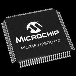
This expands on the existing line of Microchip‘s 16-bit microcontrollers, combining an expanded peripheral feature set and enhanced computational performance with a new connectivity option: USB On-The-Go. The PIC24FJ256GB110 family provides a new platform for high-performance USB applications, which may need more than an 8-bit platform, but don’t require the power of a digital signal processor.
- Power Management:
- On-Chip 2.5V Voltage Regulator
- Switch between Clock Sources in Real Time
- Idle, Sleep and Doze modes with Fast Wake-up and Two-Speed Start-up
- Run mode: 1 mA/MIPS, 2.0V Typical
- Sleep mode Current Down to 100 nA Typical
- Standby Current with 32 kHz Oscillator: 2.5 µA, 2.0V typical
- Universal Serial Bus Features:
- USB v2.0 On-The-Go (OTG) Compliant
- Dual Role Capable – can act as either Host or Peripheral
- Low-Speed (1.5 Mb/s) and Full-Speed (12 Mb/s) USB Operation in Host mode
- Full-Speed USB Operation in Device mode
- High-Precision PLL for USB
- Internal Voltage Boost Assist for USB Bus Voltage Generation
- Interface for Off-Chip Charge Pump for USB Bus Voltage Generation
- Supports up to 32 Endpoints (16 bidirectional):
- USB Module can use any RAM location on the device as USB endpoint buffers
- On-Chip USB Transceiver with On-Chip Voltage Regulator
- Interface for Off-Chip USB Transceiver
- Supports Control, Interrupt, Isochronous and Bulk Transfers
- On-Chip Pull-up and Pull-Down Resistors
- High-Performance CPU:
- Modified Harvard Architecture
- Up to 16 MIPS Operation at 32 MHz
- 8 MHz Internal Oscillator
- 17-Bit x 17-Bit Single-Cycle Hardware Multiplier
- 32-Bit by 16-Bit Hardware Divider
- 16 x 16-Bit Working Register Array
- C Compiler Optimized Instruction Set Architecture with Flexible Addressing modes
- Linear Program Memory Addressing, Up to 12 Mbytes
- Linear Data Memory Addressing, Up to 64 Kbytes
- Two Address Generation Units for Separate Read and Write Addressing of Data Memory
- Analog Features:
- 10-Bit, Up to 16-Channel Analog-to-Digital (A/D) Converter at 500 ksps:
- Conversions available in Sleep mode
- Three Analog Comparators with Programmable Input/ Output Configuration
- Charge Time Measurement Unit (CTMU)
- Peripheral Features:
- Peripheral Pin Select (PPS):
- Allows independent I/O mapping of many peripherals at run time
- Continuous hardware integrity checking and safety interlocks prevent unintentional configuration changes
- Up to 44 available pins (100-pin devices)
- Three 3-Wire/4-Wire SPI modules (supports 4 Frame modes) with 8-Level FIFO Buffer
- Three I2C™ modules support Multi-Master/Slave modes and 7-Bit/10-Bit Addressing
- Four UART modules:
- Supports RS-485, RS-232, LIN/J2602 protocols and IrDA®
- On-chip hardware encoder/decoder for IrDA
- Auto-wake-up and Auto-Baud Detect (ABD)
- 4-level deep FIFO buffer
- Five 16-Bit Timers/Counters with Programmable Prescaler
- Nine 16-Bit Capture Inputs, each with a Dedicated Time Base
- Nine 16-Bit Compare/PWM Outputs, each with a Dedicated Time Base
- 8-Bit Parallel Master Port (PMP/PSP):
- Up to 16 address pins
- Programmable polarity on control lines
- Hardware Real-Time Clock/Calendar (RTCC):
- Provides clock, calendar and alarm functions
- Programmable Cyclic Redundancy Check (CRC) Generator
- Up to 5 External Interrupt Sources
- Special Microcontroller Features:
- Operating Voltage Range of 2.0V to 3.6V
- Self-Reprogrammable under Software Control
- 5.5V Tolerant Input (digital pins only)
- Configurable Open-Drain Outputs on Digital I/O
- High-Current Sink/Source (18 mA/18 mA) on all I/O
- Selectable Power Management modes:
- Sleep, Idle and Doze modes with fast wake-up


