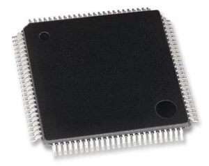
MCU 16-bit PIC24 PIC RISC 128KB Flash 2.5V/3.3V 100-Pin TQFP Tray, PIC24FJ128GA010-I/PF, Microchip

This family introduces a new line of Microchip devices: a 16-bit RISC microcontroller family with a broad peripheral feature set and enhanced computational performance. The PIC24FJ128GA family offers a new migration option for those high-performance applications which may be outgrowing their 8-bit platforms, but don’t require the numerical processing power of a digital signal processor. Core Features 16-BIT ARCHITECTURE Central to all PIC24 devices is the 16-bit modified Harvard architecture, first introduced with Microchip’s dsPIC digital signal controllers. The PIC24 CPU core offers a wide range of enhancements, such as: 16-bit data and 24-bit address paths, with the ability to move information between data and memory spaces Linear addressing of up to 8 Mbytes (program space) and 64 Kbytes (data) A 16-element working register array with built-in software stack support A 17 x 17 hardware multiplier with support for integer math Hardware support for 32 by 16-bit division An instruction set that supports multiple addressing modes and is optimized for high-level languages such as ‘C’ Operational performance up to 16 MIPS POWER-SAVING TECHNOLOGY All of the devices in the PIC24FJ128GA family incorporate a range of features that can significantly reduce power consumption during operation. Key items include: On-the-Fly Clock Switching: The device clock can be changed under software control to the Timer1 source or the internal low-power RC oscillator during operation, allowing the user to incorporate power-saving ideas into their software designs. Doze Mode Operation: When timing-sensitive applications, such as serial communications, require the uninterrupted operation of peripherals, the CPU clock speed can be selectively reduced, allowing incremental power savings without missing a beat. Instruction-Based Power-Saving Modes: The microcontroller can suspend all operations, or selectively shut down its core while leaving its peripherals active, with a single instruction in software. OSCILLATOR OPTIONS AND FEATURES All of the devices in the PIC24FJ128GA family offer five different oscillator options, allowing users a range of choices in developing application hardware. These include: Two Crystal modes, using crystals or ceramic resonators. Two External Clock modes, offering the option of a divide-by-2 clock output. A Fast Internal Oscillator (FRC) with a nominal 8 MHz output, which can also be divided under software control to provide clock speeds as low as 31 kHz. A Phase Lock Loop (PLL) frequency multiplier, available to the external oscillator modes and the FRC oscillator, which allows clock speeds of up to 32 MHz. A separate internal RC oscillator (LPRC) with a fixed 31 kHz output, which provides a low-power option for timing-insensitive applications. The internal oscillator block also provides a stable reference source for the Fail-Safe Clock Monitor. This option constantly monitors the main clock source against a reference signal provided by the internal oscillator and enables the controller to switch to the internal oscillator, allowing for continued low-speed operation or a safe application shutdown.

  • High-Performance CPU:
  • Modified Harvard Architecture
  • Up to 16 MIPS operation @ 32 MHz
  • 8 MHz internal oscillator:
    • 4x PLL option
    • Multiple divide options
  • 17-bit x 17-bit Single-Cycle Hardware Fractional/Integer Multiplier
  • 32-bit by 16-bit Hardware Divider
  • 16 x 16-bit Working Register Array
  • C compiler Optimized Instruction Set Architecture:
    • 76 base instructions
    • Flexible addressing modes
  • Linear Program Memory Addressing up to 12 Mbytes
  • Linear Data Memory Addressing up to 64 Kbytes
  • Two Address Generation Units for separate Read and Write Addressing of Data Memory
  • Special Microcontroller Features:
  • Operating Voltage Range of 2.0V to 3.6V
  • Flash Program Memory:
    • 1000 erase/write cycles, typical
    • Flash retention 20 years, typical
  • Self-Reprogrammable under Software Control
  • Selectable Power Management modes:
    • Sleep, Idle and Alternate Clock modes
  • Fail-Safe Clock Monitor operation:
    • Detects clock failure and switches to on-chip, low-power RC oscillator
  • On-Chip LDO Regulator
  • JTAG Boundary Scan and Programming Support
  • Power-on Reset (POR), Power-up Timer (PWRT) and Oscillator Start-up Timer (OST)
  • Flexible Watchdog Timer (WDT) with On-Chip, Low-Power RC Oscillator for reliable operation
  • In-Circuit Serial Programming™ (ICSP™) and In-Circuit Emulation (ICE) via 2 pins
  • Analog Features:
  • 10-bit, up to 16-channel Analog-to-Digital Converter (A/D):
    • 500 ksps conversion rate
    • Conversion available during Sleep and Idle
  • Dual Analog Comparators with Programmable Input/Output Configuration
  • Peripheral Features:
  • Two 3-wire/4-wire SPI modules, supporting 4 Frame modes with 4-level FIFO Buffer
  • Two I2C™ modules support Multi-Master/Slave mode and 7-bit/10-bit Addressing
  • Two UART modules:
    • Supports RS-232, RS-485 and LIN 1.2
    • Supports IrDA® with on-chip hardware endec
    • Auto-Wake-up on Start bit
    • Auto-Baud Detect
    • 4-level FIFO buffer
  • Parallel Master Slave Port (PMP/PSP):
    • Supports 8-bit or 16-bit data
    • Supports 16 address lines
  • Hardware Real-Time Clock/Calendar (RTCC):
    • Provides clock, calendar and alarm functions
  • Five 16-bit Timers/Counters with Programmable prescaler
  • Five 16-bit Capture Inputs
  • Five 16-bit Compare/PWM Outputs
  • High-Current Sink/Source on select I/O pins: 18 mA/18 mA
  • Configurable Open-Drain Output on Digital I/O pins
  • Up to 5 External Interrupt Sources

Характеристики

Schedule_b

8542310000

Operating_supply_voltage

2.5, 3.3 V

Operating_temperature

-40 to 85 °C

Pin_count

100

Product_dimensions

14 x 14 x 1 mm

Program_memory_size

128 KB

Ram_size

8 KB

Screening_level

Industrial

On_chip_adc

16-chx10-bit

Specifications

https://4donline.ihs.com/images/VipMasterIC/IC/MCHP/MCHP-S-A0000207333/MCHP-S-A0000207333-1.pdf?hkey=52A5661711E402568146F3353EA87419

Supplier_package

TQFP

Max_speed

16 MHz

Number_of_timers

5

Бренд

Instruction_set_architecture

RISC

Country_of_origin

China

Data_bus_width

16 Bit

Device_core

PIC

Eccn

3A991.A.2

Htsn

8542310001

Тип интерфейса

I2C/SPI/UART

Number_of_programmable_i_os

54

Lead_finish

Matte Tin

Max_operating_supply_voltage

3.6 V

Max_processing_temp

260

Min_operating_supply_voltage

2 V

Mounting

Surface Mount

Msl_level

3

Артикул: PIC24FJ128GA010-I/PF

Описание

This family introduces a new line of Microchip devices: a 16-bit RISC microcontroller family with a broad peripheral feature set and enhanced computational performance. The PIC24FJ128GA family offers a new migration option for those high-performance applications which may be outgrowing their 8-bit platforms, but don’t require the numerical processing power of a digital signal processor. Core Features 16-BIT ARCHITECTURE Central to all PIC24 devices is the 16-bit modified Harvard architecture, first introduced with Microchip’s dsPIC digital signal controllers. The PIC24 CPU core offers a wide range of enhancements, such as: 16-bit data and 24-bit address paths, with the ability to move information between data and memory spaces Linear addressing of up to 8 Mbytes (program space) and 64 Kbytes (data) A 16-element working register array with built-in software stack support A 17 x 17 hardware multiplier with support for integer math Hardware support for 32 by 16-bit division An instruction set that supports multiple addressing modes and is optimized for high-level languages such as ‘C’ Operational performance up to 16 MIPS POWER-SAVING TECHNOLOGY All of the devices in the PIC24FJ128GA family incorporate a range of features that can significantly reduce power consumption during operation. Key items include: On-the-Fly Clock Switching: The device clock can be changed under software control to the Timer1 source or the internal low-power RC oscillator during operation, allowing the user to incorporate power-saving ideas into their software designs. Doze Mode Operation: When timing-sensitive applications, such as serial communications, require the uninterrupted operation of peripherals, the CPU clock speed can be selectively reduced, allowing incremental power savings without missing a beat. Instruction-Based Power-Saving Modes: The microcontroller can suspend all operations, or selectively shut down its core while leaving its peripherals active, with a single instruction in software. OSCILLATOR OPTIONS AND FEATURES All of the devices in the PIC24FJ128GA family offer five different oscillator options, allowing users a range of choices in developing application hardware. These include: Two Crystal modes, using crystals or ceramic resonators. Two External Clock modes, offering the option of a divide-by-2 clock output. A Fast Internal Oscillator (FRC) with a nominal 8 MHz output, which can also be divided under software control to provide clock speeds as low as 31 kHz. A Phase Lock Loop (PLL) frequency multiplier, available to the external oscillator modes and the FRC oscillator, which allows clock speeds of up to 32 MHz. A separate internal RC oscillator (LPRC) with a fixed 31 kHz output, which provides a low-power option for timing-insensitive applications. The internal oscillator block also provides a stable reference source for the Fail-Safe Clock Monitor. This option constantly monitors the main clock source against a reference signal provided by the internal oscillator and enables the controller to switch to the internal oscillator, allowing for continued low-speed operation or a safe application shutdown.

  • High-Performance CPU:
  • Modified Harvard Architecture
  • Up to 16 MIPS operation @ 32 MHz
  • 8 MHz internal oscillator:
    • 4x PLL option
    • Multiple divide options
  • 17-bit x 17-bit Single-Cycle Hardware Fractional/Integer Multiplier
  • 32-bit by 16-bit Hardware Divider
  • 16 x 16-bit Working Register Array
  • C compiler Optimized Instruction Set Architecture:
    • 76 base instructions
    • Flexible addressing modes
  • Linear Program Memory Addressing up to 12 Mbytes
  • Linear Data Memory Addressing up to 64 Kbytes
  • Two Address Generation Units for separate Read and Write Addressing of Data Memory
  • Special Microcontroller Features:
  • Operating Voltage Range of 2.0V to 3.6V
  • Flash Program Memory:
    • 1000 erase/write cycles, typical
    • Flash retention 20 years, typical
  • Self-Reprogrammable under Software Control
  • Selectable Power Management modes:
    • Sleep, Idle and Alternate Clock modes
  • Fail-Safe Clock Monitor operation:
    • Detects clock failure and switches to on-chip, low-power RC oscillator
  • On-Chip LDO Regulator
  • JTAG Boundary Scan and Programming Support
  • Power-on Reset (POR), Power-up Timer (PWRT) and Oscillator Start-up Timer (OST)
  • Flexible Watchdog Timer (WDT) with On-Chip, Low-Power RC Oscillator for reliable operation
  • In-Circuit Serial Programming™ (ICSP™) and In-Circuit Emulation (ICE) via 2 pins
  • Analog Features:
  • 10-bit, up to 16-channel Analog-to-Digital Converter (A/D):
    • 500 ksps conversion rate
    • Conversion available during Sleep and Idle
  • Dual Analog Comparators with Programmable Input/Output Configuration
  • Peripheral Features:
  • Two 3-wire/4-wire SPI modules, supporting 4 Frame modes with 4-level FIFO Buffer
  • Two I2C™ modules support Multi-Master/Slave mode and 7-bit/10-bit Addressing
  • Two UART modules:
    • Supports RS-232, RS-485 and LIN 1.2
    • Supports IrDA® with on-chip hardware endec
    • Auto-Wake-up on Start bit
    • Auto-Baud Detect
    • 4-level FIFO buffer
  • Parallel Master Slave Port (PMP/PSP):
    • Supports 8-bit or 16-bit data
    • Supports 16 address lines
  • Hardware Real-Time Clock/Calendar (RTCC):
    • Provides clock, calendar and alarm functions
  • Five 16-bit Timers/Counters with Programmable prescaler
  • Five 16-bit Capture Inputs
  • Five 16-bit Compare/PWM Outputs
  • High-Current Sink/Source on select I/O pins: 18 mA/18 mA
  • Configurable Open-Drain Output on Digital I/O pins
  • Up to 5 External Interrupt Sources

Детали

Schedule_b

8542310000

Operating_supply_voltage

2.5, 3.3 V

Operating_temperature

-40 to 85 °C

Pin_count

100

Product_dimensions

14 x 14 x 1 mm

Program_memory_size

128 KB

Ram_size

8 KB

Screening_level

Industrial

On_chip_adc

16-chx10-bit

Specifications

https://4donline.ihs.com/images/VipMasterIC/IC/MCHP/MCHP-S-A0000207333/MCHP-S-A0000207333-1.pdf?hkey=52A5661711E402568146F3353EA87419

Supplier_package

TQFP

Max_speed

16 MHz

Number_of_timers

5

Бренд

Instruction_set_architecture

RISC

Country_of_origin

China

Data_bus_width

16 Bit

Device_core

PIC

Eccn

3A991.A.2

Htsn

8542310001

Тип интерфейса

I2C/SPI/UART

Number_of_programmable_i_os

54

Lead_finish

Matte Tin

Max_operating_supply_voltage

3.6 V

Max_processing_temp

260

Min_operating_supply_voltage

2 V

Mounting

Surface Mount

Msl_level

3