Описание
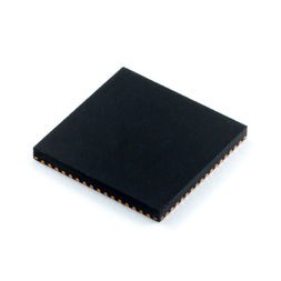
Using an “always on” ultralow-power system controller can significantly reduce power consumption on portable devices like handsets and tablets. These controllers can act as sensor hubs and monitor user stimuli (for example, reading inertial sensors or touch sensors) and vital system parameters like battery health and temperature, while power-hungry application processors and touch screen controllers are turned off. The microcontroller can then “wake up” the system based on a user input or on a fault condition that requires CPU intervention. The MSP430F525x series is the latest addition to the 1.8-V split-rail I/O portfolio (previously only available on MSP430F522x) and is specifically designed for “always on” system controller applications. 1.8-V I/O allows for seamless interface to application processors and other devices without the need for external level translation, while the primary supply to the MCU can be on a higher voltage rail. Compared to the MSP430F522x, the MSP430F525x provides up to four times more RAM (32KB) and double the serial interfaces (four USCI_A and four USCI_B). The MSP430F525x also features four 16-bit timers, a high-performance 10-bit analog-to-digital converter (ADC), a hardware multiplier, DMA, a comparator, and a real-time clock module with alarm capabilities. The MSP430F525x consumes 290 µA/MHz (typical) in active mode running from flash memory, and it consumes 1.6 µA (typical) in standby mode (LPM3). The MSP430F525x can switch to active mode in 3.5 µs (typical), which makes it a great fit for always-on low-power applications. Key benefits of the MSP430F525x are as follows: Up to 32KB RAM allows complex sensor hub algorithms and high levels of aggregation such as keyboard control and power management. Four USCI_A and four USCI_B allow for eight concurrent dedicated hardware serial interfaces (for example, four I2C and four SPI) for fast and robust communication to sensors or peripheral devices. Up to 35 I/Os that can be used in the 1.8-V voltage rail. Typical applications include analog and digital sensor fusion systems, data loggers, and various general-purpose applications.
- Primary Supply (AVCC, DVCC)
- Powered From External Supply: 3.6 V Down to 1.8 V
- Up to 18 General-Purpose I/Os With up to Eight External Interrupts
- Low-Voltage Interface Supply (DVIO)
- Powered From Separate External Supply: 1.62 V to 1.98 V
- Up to 35 General-Purpose I/Os With up to Sixteen External Interrupts
- Serial Communications
- Active Mode (AM): All System Clocks Active
290 µA/MHz at 8 MHz, 3.0 V, Flash Program Execution (Typical)
150 µA/MHz at 8 MHz, 3.0 V, RAM Program Execution (Typical) - Standby Mode (LPM3): Real-Time Clock With Crystal, Watchdog, and Supply Supervisor Operational, Full RAM Retention, Fast Wake-Up:
2.1 µA at 2.2 V, 2.3 µA at 3.0 V (Typical)
Low-Power Oscillator (VLO), General-Purpose Counter, Watchdog, and Supply Supervisor Operational, Full RAM Retention, Fast Wake-Up:
1.6 µA at 3.0 V (Typical) - Off Mode (LPM4): Full RAM Retention, Supply Supervisor Operational, Fast Wake-Up:
1.3 µA at 3.0 V (Typical) - Shutdown Mode (LPM4.5):
0.18 µA at 3.0 V (Typical)
- Fully Integrated LDO With Programmable Regulated Core Supply Voltage
- Supply Voltage Supervision, Monitoring, and Brownout
- FLL Control Loop for Frequency Stabilization
- Low-Power Low-Frequency Internal Clock Source (VLO)
- Low-Frequency Trimmed Internal Reference Source (REFO)
- 32-kHz Watch Crystals (XT1)
- HF Crystals up to 32 MHz (XT2)
- USCI_A0, A1, A2, A3 Each Support:
- Enhanced UART With Auto-Baudrate Detection
- IrDA Encoder and Decoder
- Synchronous SPI
- USCI_B0, B1, B2, B3 Each Support:
- I2C
- Synchronous SPI
- 10-Bit Analog-to-Digital Converter (ADC) With Internal Reference, Sample-and-Hold
- Comparator
- Hardware Multiplier Supports 32-Bit Operations
- Serial Onboard Programming, No External Programming Voltage Needed
- Three-Channel Internal DMA
- Basic Timer With Real-Time Clock Feature