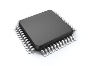
MCU 16-Bit ML620Q nX-U16/100 RISC 64KB Flash 3.3V/5V 48-Pin TQFP T/R, ML620Q504H-NNNTBWABL, ROHM

This LSI family is a high-performance 16-bit CMOS microcontroller into which rich peripheral circuits, such as synchronous serial port, UART, I2 C bus interface (master), supply voltage level detect circuit, RC oscillation type A/D converter, and successive approximation type A/D converter are incorporated around 16-bit CPU nX-U16/100. The CPU nX-U16/100 is capable of efficient instruction execution in 1-instruction 1-clock mode by 3-stage pipe line architecture parallel processing. The Flash ROM that is installed as program memory achieves low-voltage low-power consumption operation (read operation) is most suitable for battery-driven applications. And, this LSI has a data flash-memory fill area by a software which can be written in. The on-chip debug function that is installed enables program debugging and programming.

  • CPU
    • 16-bit RISC CPU (CPU name: nX-U16/100)
    • Instruction system: 16-bit instructions
    • Instruction set: Transfer, arithmetic operations, comparison, logic operations, multiplication/division, bit manipulations, bit logic operations, jump, conditional jump, call return stack manipulations, arithmetic shift, and so on
    • Build-in On-Chip debug function
    • Minimum instruction execution time 30.5 µs (@32.768 kHz system clock) 62.5ns (@16 MHz system clock)
  • Built-in coprocessor for multiplication, division, and multiply-accumulate operations
    • Signed or unsigned operation setting
    • Multiplication: 16bit x 16bit (operation time 4 cycles)
    • Division: 32bit / 16bit (operation time 8 cycles)
    • Division: 32bit / 32bit (operation time 16 cycles)
    • Multiply-accumulate (non-saturating): 16bit x 16bit + 32bit (operation time 4 cycles)
    • Multiply-accumulate (saturating): 16bit x 16bit + 32bit (operation time 4 cycles)
  • Internal memory
    • Supports ISP function (re-writing the program memory area by software)
    • Number of segments Product name Flash memory SRAM Program area* Data area ML620Q504H 64KB (32K x 16bit) 2KB (1K x 16bit) 6KB (3K x 16bit) *: including 1KB of unusable test area
  • Interrupt controller (INTC)
    • 1 non-maskable interrupt sources (Internal source: 1)
    • 37 maskable interrupt sources (Internal sources: 29, External sources: 8)
    • Software interrupt (SWI): maximum 64 sources
    • External interrupts and comparator allow edge selection and sampling selection
    • Priority level (4-level) can be set for each interrupt
  • Time base counter (TBC)
    • Low-speed time base counter x1 channel FEDL620Q504H-01 ML620Q503H/Q504H 2/35
  • Timers (TMR)
    • 8 bits x 8 channels (Timer0-7: 16-bit x 4 configuration available by using Timer0-1 or Timer2-3, Timer4-5, Timer6-7)
    • Selection of one shot timer mode is possible
    • External clock can be selected as timer clock.
  • Function Timers (FTM)
    • 16-bit x 4 channels
    • Equipped with the timer/capture/PWM functions using a 16-bit counter
    • Timer start/stop function by software/event trriger(external pin or other timer).
Характеристики

Analog_comparators

2

Max_speed

16.8 MHz

Operating_supply_voltage

3.3, 5 V

Operating_temperature

-40 to 85 °C

Pin_count

48

Product_dimensions

7 x 7 x 1 mm

Program_memory_size

8 KB

Program_memory_type

Flash

Ram_size

0.75 KB

Screening_level

Industrial

On_chip_adc

12-chx12-bit

Specifications

http://www.lapis-semi.com/en/data/datasheet-file_db/miconlp/FEDL620Q504H-01.pdf

Supplier_package

TQFP

Watchdog

1

Schedule_b

8542310000

Бренд

Number_of_timers

12

Instruction_set_architecture

RISC

Country_of_origin

Thailand

Data_bus_width

16 Bit

Data_memory_size

2 KB

Device_core

nX-U16/100

Eccn

EAR99

Htsn

8542310001

Тип интерфейса

I2C/SSP/UART/USART

Number_of_programmable_i_os

36

Max_operating_supply_voltage

5.5 V

Max_power_dissipation

900 mW

Min_operating_supply_voltage

1.8 V

Mounting

Surface Mount

Артикул: ML620Q504H-NNNTBWABL

Описание

This LSI family is a high-performance 16-bit CMOS microcontroller into which rich peripheral circuits, such as synchronous serial port, UART, I2 C bus interface (master), supply voltage level detect circuit, RC oscillation type A/D converter, and successive approximation type A/D converter are incorporated around 16-bit CPU nX-U16/100. The CPU nX-U16/100 is capable of efficient instruction execution in 1-instruction 1-clock mode by 3-stage pipe line architecture parallel processing. The Flash ROM that is installed as program memory achieves low-voltage low-power consumption operation (read operation) is most suitable for battery-driven applications. And, this LSI has a data flash-memory fill area by a software which can be written in. The on-chip debug function that is installed enables program debugging and programming.

  • CPU
    • 16-bit RISC CPU (CPU name: nX-U16/100)
    • Instruction system: 16-bit instructions
    • Instruction set: Transfer, arithmetic operations, comparison, logic operations, multiplication/division, bit manipulations, bit logic operations, jump, conditional jump, call return stack manipulations, arithmetic shift, and so on
    • Build-in On-Chip debug function
    • Minimum instruction execution time 30.5 µs (@32.768 kHz system clock) 62.5ns (@16 MHz system clock)
  • Built-in coprocessor for multiplication, division, and multiply-accumulate operations
    • Signed or unsigned operation setting
    • Multiplication: 16bit x 16bit (operation time 4 cycles)
    • Division: 32bit / 16bit (operation time 8 cycles)
    • Division: 32bit / 32bit (operation time 16 cycles)
    • Multiply-accumulate (non-saturating): 16bit x 16bit + 32bit (operation time 4 cycles)
    • Multiply-accumulate (saturating): 16bit x 16bit + 32bit (operation time 4 cycles)
  • Internal memory
    • Supports ISP function (re-writing the program memory area by software)
    • Number of segments Product name Flash memory SRAM Program area* Data area ML620Q504H 64KB (32K x 16bit) 2KB (1K x 16bit) 6KB (3K x 16bit) *: including 1KB of unusable test area
  • Interrupt controller (INTC)
    • 1 non-maskable interrupt sources (Internal source: 1)
    • 37 maskable interrupt sources (Internal sources: 29, External sources: 8)
    • Software interrupt (SWI): maximum 64 sources
    • External interrupts and comparator allow edge selection and sampling selection
    • Priority level (4-level) can be set for each interrupt
  • Time base counter (TBC)
    • Low-speed time base counter x1 channel FEDL620Q504H-01 ML620Q503H/Q504H 2/35
  • Timers (TMR)
    • 8 bits x 8 channels (Timer0-7: 16-bit x 4 configuration available by using Timer0-1 or Timer2-3, Timer4-5, Timer6-7)
    • Selection of one shot timer mode is possible
    • External clock can be selected as timer clock.
  • Function Timers (FTM)
    • 16-bit x 4 channels
    • Equipped with the timer/capture/PWM functions using a 16-bit counter
    • Timer start/stop function by software/event trriger(external pin or other timer).

Детали

Analog_comparators

2

Max_speed

16.8 MHz

Operating_supply_voltage

3.3, 5 V

Operating_temperature

-40 to 85 °C

Pin_count

48

Product_dimensions

7 x 7 x 1 mm

Program_memory_size

8 KB

Program_memory_type

Flash

Ram_size

0.75 KB

Screening_level

Industrial

On_chip_adc

12-chx12-bit

Specifications

http://www.lapis-semi.com/en/data/datasheet-file_db/miconlp/FEDL620Q504H-01.pdf

Supplier_package

TQFP

Watchdog

1

Schedule_b

8542310000

Бренд

Number_of_timers

12

Instruction_set_architecture

RISC

Country_of_origin

Thailand

Data_bus_width

16 Bit

Data_memory_size

2 KB

Device_core

nX-U16/100

Eccn

EAR99

Htsn

8542310001

Тип интерфейса

I2C/SSP/UART/USART

Number_of_programmable_i_os

36

Max_operating_supply_voltage

5.5 V

Max_power_dissipation

900 mW

Min_operating_supply_voltage

1.8 V

Mounting

Surface Mount