Описание
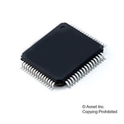
The MC56F825x is a member of the 56800E core-based family of digital signal controllers (DSCs). It combines, on a single chip, the processing power of a DSP and the functionality of a microcontroller with a flexible set of peripherals to create a cost-effective solution. Because of its low cost, configuration flexibility, and compact program code, it is well-suited for many applications. The 56800E core is based on a modified Harvard-style architecture consisting of three execution units operating in parallel, allowing as many as six operations per instruction cycle. The MCU-style programming model and optimized instruction set allow straightforward generation of efficient, compact DSP and control code. The instruction set is also highly efficient for C compilers to enable rapid development of optimized control applications. The MC56F825x supports program execution from internal memories. Two data operands per instruction cycle can be accessed from the on-chip data RAM. A full set of programmable peripherals supports various applications. Each peripheral can be independently shut down to save power. Any pin, except Power pins and the Reset pin, can also be configured as General Purpose Input/Outputs (GPIOs).
- Core
- Efficient 56800E digital signal processor (DSP) engine with modified Harvard architecture
- As many as 60 million instructions per second (MIPS) at 60 MHz core frequency
- 155 basic instructions in conjunction with up to 20 address modes
- 32-bit internal primary data buses supporting 8-bit, 16-bit, and 32-bit data movement, addition, subtraction, and logical operation
- Single-cycle 16 X 16-bit parallel multiplier-accumulator (MAC)
- Operation Range
- 3.0 V to 3.6 V operation (power supplies and I/O)
- From power-on-reset: approximately 2.7 V to 3.6 V
- Ambient temperature operating range
- Memory
- Dual Harvard architecture that permits as many as three simultaneous accesses to program and data memory
- 48 KB (24K x 16) to 64 KB (32K x 16) on-chip flash memory with 2048 bytes (1024 x 16) page size
- 6 KB (3K x 16) to 8 KB (4K x 16) on-chip RAM with byte addressable
- EEPROM emulation capability using flash
- Interrupt Controller
- Nested interrupts: higher priority level interrupt request can interrupt lower priority interrupt subroutine
- Two programmable fast interrupts that can be assigned to any interrupt source
- Notification to system integration module (SIM) to restart clock out of wait and stop states
- Ability to relocate interrupt vector table
- Peripheral Highlights
- One Enhanced Flex Pulse Width Modulator (eFlexPWM) module
- Two independent 12-bit analog-to-digital converters (ADCs)
- Inter-module Crossbar Switch (XBAR)
- Three analog comparators (CMPs)
- One 12-bit digital-to-analog converter (12-bit DAC)
- Two four-channel 16-bit multi-purpose timer (TMR) modules
- Two queued serial communication interface (QSCI) modules with LIN slave functionality
- One queued serial peripheral interface (QSPI) module
- Two inter-integrated circuit (I2 C) ports
- One Freescale Scalable Controller Area Network (MSCAN) module
- Computer operating properly (COP) watchdog timer capable of selecting different clock sources
- Power supervisor (PS)
- Phase lock loop (PLL) providing a high-speed clock to the core and peripherals
- JTAG/EOnCE debug programming interface for real-time debugging
