MCU 16-Bit HCS12 HCS12 CISC 48KB Flash 3.3V/5V 48-Pin LQFP, S9S12GN48F0WLF, NXP

The MC9S12G-Family is an optimized, automotive, 16-bit microcontroller product line focused on low-cost, high-performance, and low pin-count. This family is intended to bridge between high-end 8-bit microcontrollers and high-performance 16-bit microcontrollers, such as the MC9S12XS-Family. The MC9S12G-Family is targeted at generic automotive applications requiring CAN or LIN/J2602 communication. Typical examples of these applications include body controllers, occupant detection, door modules, seat controllers, RKE receivers, smart actuators, lighting modules, and smart junction boxes. The MC9S12G-Family uses many of the same features found on the MC9S12XS- and MC9S12P-Family, including error correction code (ECC) on flash memory, a fast analog-to-digital converter (ADC) and a frequency modulated phase locked loop (IPLL) that improves the EMC performance. The MC9S12G-Family is optimized for lower program memory sizes down to 16k. In order to simplify customer use it features an EEPROM with a small 4 bytes erase sector size. The MC9S12G-Family deliver all the advantages and efficiencies of a 16-bit MCU while retaining the low cost, power consumption, EMC, and code-size efficiency advantages currently enjoyed by users of Freescale’s existing 8-bit and 16-bit MCU families. Like the MC9S12XS-Family, the MC9S12G-Family run 16-bit wide accesses without wait states for all peripherals and memories. The MC9S12G-Family is available in 100-pin LQFP, 64-pin LQFP, 48-pin LQFP/QFN, 32-pin LQFP and 20-pin TSSOP package options and aims to maximize the amount of functionality especially for the lower pin count packages. In addition to the I/O ports available in each module, further I/O ports are available with interrupt capability allowing wake-up from stop or wait modes.

  • Chip-Level Features
    • S12 CPU core
    • Up to 240 Kbyte on-chip flash with ECC
    • Up to 4 Kbyte EEPROM with ECC
    • Up to 11 Kbyte on-chip SRAM
    • Phase locked loop (IPLL) frequency multiplier with internal filter
    • 4–16 MHz amplitude controlled Pierce oscillator
    • 1 MHz internal RC oscillator
    • Timer module (TIM) supporting up to eight channels that provide a range of 16-bit input capture, output compare, counter, and pulse accumulator functions
  • Module Features
    • Full 16-bit data paths supports efficient arithmetic operation and high-speed math execution
    • Includes many single-byte instructions. This allows much more efficient use of ROM space.
    • Up to 240 Kbyte of program flash memory
    • Up to 4 Kbyte EEPROM
    • Up to 11 Kbytes of general-purpose RAM
    • Data registers and data direction registers for ports A, B, C, D, E, T, S, M, P, J and AD when used as general-purpose I/O
    • Control registers to enable/disable pull devices and select pullups/pulldowns on ports T, S, M, P, J and AD on per-pin basis
    • Single control register to enable/disable pull devices on ports A, B, C, D and E, on per-port basis and on BKGD pin
    • Control registers to enable/disable open-drain (wired-or) mode on ports S and M
    • Loop control Pierce oscillator using a 4 MHz to 16 MHz crystal
    • Trimmable internal reference clock.
    • Phase-locked-loop clock frequency multiplier
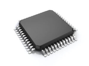
Характеристики

Analog_comparators

1

Schedule_b

8542310000

Operating_supply_voltage

3.3, 5 V

Operating_temperature

-40 to 150 °C

Pin_count

48

Product_dimensions

7 x 7 x 1.4

On_chip_adc

12-chx10-bit

Special_features

CAN Controller

Specifications

http://cache.freescale.com/files/32bit/doc/ref_manual/MC9S12GRMV1.pdf

Supplier_package

LQFP

Watchdog

1

Max_speed

25 MHz

Number_of_timers

6

Бренд

Instruction_set_architecture

CISC

Country_of_origin

China

Data_bus_width

16 Bit

Data_memory_size

1.5 KB

Device_core

S12

Eccn

3A991.A.2

Htsn

8542310001

Тип интерфейса

CAN/SCI/SPI

Number_of_programmable_i_os

40

Lead_finish

Matte Tin

Max_processing_temp

260

Mounting

Surface Mount

Msl_level

3

Артикул: S9S12GN48F0WLF

Описание

The MC9S12G-Family is an optimized, automotive, 16-bit microcontroller product line focused on low-cost, high-performance, and low pin-count. This family is intended to bridge between high-end 8-bit microcontrollers and high-performance 16-bit microcontrollers, such as the MC9S12XS-Family. The MC9S12G-Family is targeted at generic automotive applications requiring CAN or LIN/J2602 communication. Typical examples of these applications include body controllers, occupant detection, door modules, seat controllers, RKE receivers, smart actuators, lighting modules, and smart junction boxes. The MC9S12G-Family uses many of the same features found on the MC9S12XS- and MC9S12P-Family, including error correction code (ECC) on flash memory, a fast analog-to-digital converter (ADC) and a frequency modulated phase locked loop (IPLL) that improves the EMC performance. The MC9S12G-Family is optimized for lower program memory sizes down to 16k. In order to simplify customer use it features an EEPROM with a small 4 bytes erase sector size. The MC9S12G-Family deliver all the advantages and efficiencies of a 16-bit MCU while retaining the low cost, power consumption, EMC, and code-size efficiency advantages currently enjoyed by users of Freescale’s existing 8-bit and 16-bit MCU families. Like the MC9S12XS-Family, the MC9S12G-Family run 16-bit wide accesses without wait states for all peripherals and memories. The MC9S12G-Family is available in 100-pin LQFP, 64-pin LQFP, 48-pin LQFP/QFN, 32-pin LQFP and 20-pin TSSOP package options and aims to maximize the amount of functionality especially for the lower pin count packages. In addition to the I/O ports available in each module, further I/O ports are available with interrupt capability allowing wake-up from stop or wait modes.

  • Chip-Level Features
    • S12 CPU core
    • Up to 240 Kbyte on-chip flash with ECC
    • Up to 4 Kbyte EEPROM with ECC
    • Up to 11 Kbyte on-chip SRAM
    • Phase locked loop (IPLL) frequency multiplier with internal filter
    • 4–16 MHz amplitude controlled Pierce oscillator
    • 1 MHz internal RC oscillator
    • Timer module (TIM) supporting up to eight channels that provide a range of 16-bit input capture, output compare, counter, and pulse accumulator functions
  • Module Features
    • Full 16-bit data paths supports efficient arithmetic operation and high-speed math execution
    • Includes many single-byte instructions. This allows much more efficient use of ROM space.
    • Up to 240 Kbyte of program flash memory
    • Up to 4 Kbyte EEPROM
    • Up to 11 Kbytes of general-purpose RAM
    • Data registers and data direction registers for ports A, B, C, D, E, T, S, M, P, J and AD when used as general-purpose I/O
    • Control registers to enable/disable pull devices and select pullups/pulldowns on ports T, S, M, P, J and AD on per-pin basis
    • Single control register to enable/disable pull devices on ports A, B, C, D and E, on per-port basis and on BKGD pin
    • Control registers to enable/disable open-drain (wired-or) mode on ports S and M
    • Loop control Pierce oscillator using a 4 MHz to 16 MHz crystal
    • Trimmable internal reference clock.
    • Phase-locked-loop clock frequency multiplier
Детали

Analog_comparators

1

Schedule_b

8542310000

Operating_supply_voltage

3.3, 5 V

Operating_temperature

-40 to 150 °C

Pin_count

48

Product_dimensions

7 x 7 x 1.4

On_chip_adc

12-chx10-bit

Special_features

CAN Controller

Specifications

http://cache.freescale.com/files/32bit/doc/ref_manual/MC9S12GRMV1.pdf

Supplier_package

LQFP

Watchdog

1

Max_speed

25 MHz

Number_of_timers

6

Бренд

Instruction_set_architecture

CISC

Country_of_origin

China

Data_bus_width

16 Bit

Data_memory_size

1.5 KB

Device_core

S12

Eccn

3A991.A.2

Htsn

8542310001

Тип интерфейса

CAN/SCI/SPI

Number_of_programmable_i_os

40

Lead_finish

Matte Tin

Max_processing_temp

260

Mounting

Surface Mount

Msl_level

3