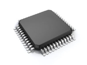
MCU 16-bit HCS12 HC12 CISC 32KB Flash 9V/12V/15V 48-Pin LQFP EP T/R, MM912F634DV2AER2, NXP

The MM912G634 (48 kB) and MM912H634 (64 kB) are integrated single package solutions that integrate an HCS12 MCU with a SMARTMOS analog control IC. The Die to Die Interface (D2D) controlled analog die combines system base chip and application-specific functions, including a LIN transceiver. Your customer benefits include: Integrated MCU and analog features in the same package solution A full LIN solution Easy control of high-current motors using relays and current sense features Reduced space, resulting in enhanced reliability Full protection for output stages Economical multifunction solution with few components Low-power mode flexibility Reverse-battery-protected voltage sense

CPU Core

  • 16-Bit S12 CPU, 64/48/32 kByte Program Flash
  • 4/2/0 kByte Data Flash
  • 6/2/2 kBytes of RAM
  • Background debug (BDM) & debug module (DBG)
  • 16-Bit, 4 Channel – Timer Module (TIM16B4C)
  • Die to Die bus interface for transparent memory mapping

Standard I/O

  • 6 or 10 digital MCU GPIOs shared with SPI
  • 10-Bit, 15 Channel – Analog to Digital Converter (ADC)
  • 8-Bit, 2 Channel – Pulse width modulation module (PWM)

Application Specific Functions

  • On-chip oscillator & two independent watchdogs
  • LIN 2.1 Physical Layer Interface with integrated SCI
  • Six high voltage / Wake-up inputs (L5…0)
  • Three low voltage GPIOs (PB2…0)
  • Low power modes with cyclic sense & forced wake-up
  • Two protected low side outputs to drive inductive loads
  • Two protected high side outputs
  • Hall sensor supply & integrated voltage regulator(s)
  • Reverse battery protected voltage sense module
  • Chip temperature sensor
  • Current sense module with selectable gain
Характеристики

Schedule_b

8542390000

Бренд

Operating_temperature

-40 to 105 °C

Pin_count

48

Product_dimensions

7 x 7 x 1.4

Program_memory_size

32 Kb

Ram_size

2 KB

On_chip_adc

15-chx10-bit

Specifications

https://4donline.ihs.com/images/VipMasterIC/IC/PHGL/PHGL-S-A0006172384/PHGL-S-A0006172384-1.pdf?hkey=52A5661711E402568146F3353EA87419

Supplier_package

LQFP EP

Watchdog

2

Max_speed

20 MHz

Number_of_timers

4

Operating_supply_voltage

9, 12, 15 V

Country_of_origin

China

Instruction_set_architecture

CISC

Data_bus_width

16 Bit

Device_core

HC12

Eccn

3A991.A.2

Htsn

8542390001

Тип интерфейса

SCI/SPI

Number_of_programmable_i_os

9

Lead_finish

Matte Tin

Max_operating_supply_voltage

18 V

Max_processing_temp

260 °C

Min_operating_supply_voltage

5.5 V

Mounting

Surface Mount

Msl_level

3

Артикул: MM912F634DV2AER2

Описание

The MM912G634 (48 kB) and MM912H634 (64 kB) are integrated single package solutions that integrate an HCS12 MCU with a SMARTMOS analog control IC. The Die to Die Interface (D2D) controlled analog die combines system base chip and application-specific functions, including a LIN transceiver. Your customer benefits include: Integrated MCU and analog features in the same package solution A full LIN solution Easy control of high-current motors using relays and current sense features Reduced space, resulting in enhanced reliability Full protection for output stages Economical multifunction solution with few components Low-power mode flexibility Reverse-battery-protected voltage sense

CPU Core

  • 16-Bit S12 CPU, 64/48/32 kByte Program Flash
  • 4/2/0 kByte Data Flash
  • 6/2/2 kBytes of RAM
  • Background debug (BDM) & debug module (DBG)
  • 16-Bit, 4 Channel – Timer Module (TIM16B4C)
  • Die to Die bus interface for transparent memory mapping

Standard I/O

  • 6 or 10 digital MCU GPIOs shared with SPI
  • 10-Bit, 15 Channel – Analog to Digital Converter (ADC)
  • 8-Bit, 2 Channel – Pulse width modulation module (PWM)

Application Specific Functions

  • On-chip oscillator & two independent watchdogs
  • LIN 2.1 Physical Layer Interface with integrated SCI
  • Six high voltage / Wake-up inputs (L5…0)
  • Three low voltage GPIOs (PB2…0)
  • Low power modes with cyclic sense & forced wake-up
  • Two protected low side outputs to drive inductive loads
  • Two protected high side outputs
  • Hall sensor supply & integrated voltage regulator(s)
  • Reverse battery protected voltage sense module
  • Chip temperature sensor
  • Current sense module with selectable gain

Детали

Schedule_b

8542390000

Бренд

Operating_temperature

-40 to 105 °C

Pin_count

48

Product_dimensions

7 x 7 x 1.4

Program_memory_size

32 Kb

Ram_size

2 KB

On_chip_adc

15-chx10-bit

Specifications

https://4donline.ihs.com/images/VipMasterIC/IC/PHGL/PHGL-S-A0006172384/PHGL-S-A0006172384-1.pdf?hkey=52A5661711E402568146F3353EA87419

Supplier_package

LQFP EP

Watchdog

2

Max_speed

20 MHz

Number_of_timers

4

Operating_supply_voltage

9, 12, 15 V

Country_of_origin

China

Instruction_set_architecture

CISC

Data_bus_width

16 Bit

Device_core

HC12

Eccn

3A991.A.2

Htsn

8542390001

Тип интерфейса

SCI/SPI

Number_of_programmable_i_os

9

Lead_finish

Matte Tin

Max_operating_supply_voltage

18 V

Max_processing_temp

260 °C

Min_operating_supply_voltage

5.5 V

Mounting

Surface Mount

Msl_level

3