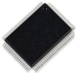
MCU 16-bit H8S CISC 128KB Flash 5V 100-Pin PQFP Tray, DF2144AFA20V, Renesas Electronics

This LSI comprise microcomputers (MCUs) built around the H8S/2000 CPU, employing Renesas Technology proprietary architecture, and equipped with supporting modules on-chip. The H8S/2000 CPU has an internal 32-bit architecture, is provided with sixteen 16-bit general registers and a concise, optimized instruction set designed for high-speed operation, and can address a 16-Mbyte linear address space. The instruction set is upward-compatible with H8/300 and H8/300H CPU instructions at the object-code level, facilitating migration from the H8/300, H8/300L, or H8/300H Series. On-chip supporting modules required for system configuration include a data transfer controller (DTC) bus master, ROM and RAM, a 16-bit free-running timer module (FRT), 8-bit timer module (TMR), watchdog timer module (WDT), two PWM timers (PWM and PWMX), serial communication interface (SCI), PS/2-compatible keyboard buffer controller, host interface (HIF), D/A converter (DAC), A/D converter (ADC), and I/O ports. An I2 C bus interface (IIC) can also be incorporated as an option. The on-chip ROM is either flash memory (F-ZTAT*) or mask ROM, with a capacity of 128, 96, or 64 kbytes. ROM is connected to the CPU via a 16-bit data bus, enabling both byte and word data to be accessed in one state. Instruction fetching has been speeded up, and processing speed increased. Three operating modes, modes 1 to 3, are provided, and there is a choice of address space and single-chip mode or externally expanded modes.

  • General-register architecture
    • Sixteen 16-bit general registers (also usable as sixteen 8-bit registers or eight 32-bit registers)
  • High-speed operation suitable for real-time control
    • Maximum operating frequency: 20 MHz/5 V, 10 MHz/3 V
    • High-speed arithmetic operations 8/16/32-bit register-register add/subtract: 50 ns (20-MHz operation) 16 × 16-bit register-register multiply: 1000 ns (20-MHz operation) 32 ÷ 16-bit register-register divide: 1000 ns (20-MHz operation)
  • Instruction set suitable for high-speed operation
    • Sixty-five basic instructions
    • 8/16/32-bit transfer/arithmetic and logic instructions
    • Unsigned/signed multiply and divide instructions
    • Powerful bit-manipulation instructions
  • Two CPU operating modes
    • Normal mode: 64-kbyte address space
    • Advanced mode: 16-Mbyte address space
Характеристики

Schedule_b

8542310000

Number_of_timers

4

Operating_temperature

-20 to 75 °C

Pin_count

100

Product_dimensions

14 x 14 x 2.7 mm

Program_memory_size

128 KB

Ram_size

4 KB

On_chip_adc

16-chx10-bit

Specifications

https://4donline.ihs.com/images/VipMasterIC/IC/RNCC/RNCCS11701/RNCCS11701-1.pdf?hkey=52A5661711E402568146F3353EA87419

Supplier_package

PQFP

Watchdog

1

Max_speed

20 MHz

On_chip_dac

2-chx8-bit

Operating_supply_voltage

5 V

Instruction_set_architecture

CISC

Бренд

Data_bus_width

16 Bit

Eccn

EAR99

Htsn

8542310001

Тип интерфейса

HIF/SCI

Number_of_programmable_i_os

74

Lead_finish

Gold, Tin/Bismuth, Tin/Copper

Max_expanded_memory_size

16 MB

Max_operating_supply_voltage

5.5 V

Max_processing_temp

245, 260

Min_operating_supply_voltage

4.5 V

Mounting

Surface Mount

Msl_level

3

SKU: DF2144AFA20V

Description

This LSI comprise microcomputers (MCUs) built around the H8S/2000 CPU, employing Renesas Technology proprietary architecture, and equipped with supporting modules on-chip. The H8S/2000 CPU has an internal 32-bit architecture, is provided with sixteen 16-bit general registers and a concise, optimized instruction set designed for high-speed operation, and can address a 16-Mbyte linear address space. The instruction set is upward-compatible with H8/300 and H8/300H CPU instructions at the object-code level, facilitating migration from the H8/300, H8/300L, or H8/300H Series. On-chip supporting modules required for system configuration include a data transfer controller (DTC) bus master, ROM and RAM, a 16-bit free-running timer module (FRT), 8-bit timer module (TMR), watchdog timer module (WDT), two PWM timers (PWM and PWMX), serial communication interface (SCI), PS/2-compatible keyboard buffer controller, host interface (HIF), D/A converter (DAC), A/D converter (ADC), and I/O ports. An I2 C bus interface (IIC) can also be incorporated as an option. The on-chip ROM is either flash memory (F-ZTAT*) or mask ROM, with a capacity of 128, 96, or 64 kbytes. ROM is connected to the CPU via a 16-bit data bus, enabling both byte and word data to be accessed in one state. Instruction fetching has been speeded up, and processing speed increased. Three operating modes, modes 1 to 3, are provided, and there is a choice of address space and single-chip mode or externally expanded modes.

  • General-register architecture
    • Sixteen 16-bit general registers (also usable as sixteen 8-bit registers or eight 32-bit registers)
  • High-speed operation suitable for real-time control
    • Maximum operating frequency: 20 MHz/5 V, 10 MHz/3 V
    • High-speed arithmetic operations 8/16/32-bit register-register add/subtract: 50 ns (20-MHz operation) 16 × 16-bit register-register multiply: 1000 ns (20-MHz operation) 32 ÷ 16-bit register-register divide: 1000 ns (20-MHz operation)
  • Instruction set suitable for high-speed operation
    • Sixty-five basic instructions
    • 8/16/32-bit transfer/arithmetic and logic instructions
    • Unsigned/signed multiply and divide instructions
    • Powerful bit-manipulation instructions
  • Two CPU operating modes
    • Normal mode: 64-kbyte address space
    • Advanced mode: 16-Mbyte address space
Additional information

Schedule_b

8542310000

Number_of_timers

4

Operating_temperature

-20 to 75 °C

Pin_count

100

Product_dimensions

14 x 14 x 2.7 mm

Program_memory_size

128 KB

Ram_size

4 KB

On_chip_adc

16-chx10-bit

Specifications

https://4donline.ihs.com/images/VipMasterIC/IC/RNCC/RNCCS11701/RNCCS11701-1.pdf?hkey=52A5661711E402568146F3353EA87419

Supplier_package

PQFP

Watchdog

1

Max_speed

20 MHz

On_chip_dac

2-chx8-bit

Operating_supply_voltage

5 V

Instruction_set_architecture

CISC

Бренд

Data_bus_width

16 Bit

Eccn

EAR99

Htsn

8542310001

Тип интерфейса

HIF/SCI

Number_of_programmable_i_os

74

Lead_finish

Gold, Tin/Bismuth, Tin/Copper

Max_expanded_memory_size

16 MB

Max_operating_supply_voltage

5.5 V

Max_processing_temp

245, 260

Min_operating_supply_voltage

4.5 V

Mounting

Surface Mount

Msl_level

3