Описание
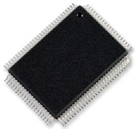
The H8/3024 Series is a series of microcontrollers (MCUs) that integrate system supporting functions together with an H8/300H CPU core having an original Hitachi architecture.The H8/300H CPU has a 32-bit internal architecture with sixteen 16-bit general registers, and a concise, optimized instruction set designed for speed. It can address a 16-Mbyte linear address space. Its instruction set is upward-compatible at the object-code level with the H8/300 CPU, enabling easy porting of software from the H8/300 Series.The on-chip system supporting functions include ROM, RAM, a 16-bit timer, an 8-bit timer, a programmable timing pattern controller (TPC), a watchdog timer (WDT), a serial communication interface (SCI), an A/D converter, a D/A converter, I/O ports, and other facilities.The four members of the H8/3024 Series are the H8/3024F-ZTAT, H8/3026F-ZTAT, H8/3024 (mask ROM version), and H8/3026 (mask ROM version).Seven MCU operating modes offer a choice of bus width and address space size. The modes (modes 1 to 7) include two single-chip modes and five expanded modes.In addition to its mask ROM versions, the H8/3024 Series has F-ZTAT versions with on-chip flash memory that allows programs to be freely rewritten by the user. This version enables users to respond quickly and flexibly to changing application specifications, growing production volumes, and other conditions.
- Sixteen 16-bit general registers (also usable as sixteen 8-bit registers plus eight 16-bit registers, or as eight 32-bit registers)
- 16-Mbyte address space
- 8/16/32-bit data transfer, arithmetic, and logic instructions
- Signed and unsigned multiply instructions (8 bits x 8 bits, 16 bits x 16 bits)
- Signed and unsigned divide instructions (16 bits ÷ 8 bits, 32 bits ÷ 16 bits)
- Bit accumulator function
- Seven external interrupt pins: NMI, IRQ0 to IRQ5
- 27 internal interrupts
- Three selectable interrupt priority levels