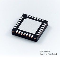
MCU 16-bit dSPIC33 dsPIC RISC 128KB Flash 3.3V 28-Pin QFN-S EP T/R, DSPIC33FJ128GP202T-I/MM, Microchip

16-Bit Digital Signal Controllers (up to 32-Kbyte Flash and 2-Kbyte SRAM)

Operating Conditions • 3.0V to 3.6V, -40°C to +125°C, DC to 16 MIPS • 3.0V to 3.6V, -40°C to +150°C, DC to 5 MIPS Core: 16-Bit dsPIC33F CPU • Code-Efficient (C and Assembly) Architecture • Two 40-Bit Wide Accumulators • Single-Cycle (MAC/MPY) with Dual Data Fetch • Single-Cycle Mixed-Sign MUL plus Hardware Divide • 32-Bit Multiply Support Clock Management • ±0.25% Internal Oscillator • Programmable PLLs and Oscillator Clock Sources • Fail-Safe Clock Monitor (FSCM) • Independent Watchdog Timer (WDT) • Fast Wake-up and Start-up Power Management • Low-Power Management modes (Sleep, Idle, Doze) • Integrated Power-on Reset and Brown-out Reset • 1 mA/MHz Dynamic Current (typical) • 30 µA IPD Current (typical) PWM • Up to Three PWM Pairs • Two Dead-Time Generators • 31.25 ns PWM Resolution • PWM Support for: – Inverters, PFC, UPS – BLDC, PMSM, ACIM, SRM • Class B-Compliant Fault Inputs • Possibility of ADC Synchronization with PWM Signal Advanced Analog Features • ADC module: – 10-bit, 1.1 Msps with four S&H – Four analog inputs on 18-pin devices and up to 14 analog inputs on 44-pin devices • Flexible and Independent ADC Trigger Sources • Three Comparator modules • Charge Time Measurement Unit (CTMU): – Supports mTouch™ capacitive touch sensing – Provides high-resolution time measurement (1 ns) – On-chip temperature measurement Timers/Output Compare/Input Capture • Up to Five General Purpose Timers: – One 16-bit and up to two 32-bit timers/counters • Two Output Compare modules • Three Input Capture modules • Peripheral Pin Select (PPS) to allow Function Remap Communication Interfaces • UART module (4 Mbps): – With support for LIN/J2602 Protocols and IrDA® • 4-Wire SPI module (8 MHz maximum speed): – Remappable pins in 32-Kbyte Flash devices • I2C™ module (400 kHz) Input/Output • Sink/Source 10 mA or 6 mA, Pin-Specific for Standard VOH/VOL, up to 16 mA or 12 mA for Non-Standard VOH1 • 5V Tolerant Pins • Up to 20 Selectable Open-Drain and Pull-ups • Three External Interrupts (two are remappable) Qualification and Class B Support • AEC-Q100 REV G (Grade 0 -40°C to +150°C) • Class B Safety Library, IEC 60730, UDE Certified Debugger Development Support • In-Circuit and In-Application Programming • Up to Three Complex Data Breakpoints • Trace and Run-Time Watch
Характеристики

Schedule_b

8542310000

Operating_supply_voltage

3.3 V

Operating_temperature

-40 to 85 °C

Pin_count

28

Product_dimensions

6 x 6 x 0.88 mm

Specifications

https://4donline.ihs.com/images/VipMasterIC/IC/MCHP/MCHPS03727/MCHPS03727-1.pdf?hkey=52A5661711E402568146F3353EA87419

Max_speed

40 MHz

On_chip_dac

2-chx16-bit

Number_of_timers

5

Бренд

Country_of_origin

Thailand

Eccn

3A991.A.2

Htsn

8542310001

Тип интерфейса

I2C/SPI/UART

Number_of_programmable_i_os

21

Lead_finish

Matte Tin

Max_operating_supply_voltage

3.6, 3.9 V

Min_operating_supply_voltage

2.7, 3 V

Mounting

Surface Mount

Артикул: DSPIC33FJ128GP202T-I/MM

Описание

16-Bit Digital Signal Controllers (up to 32-Kbyte Flash and 2-Kbyte SRAM)

Operating Conditions • 3.0V to 3.6V, -40°C to +125°C, DC to 16 MIPS • 3.0V to 3.6V, -40°C to +150°C, DC to 5 MIPS Core: 16-Bit dsPIC33F CPU • Code-Efficient (C and Assembly) Architecture • Two 40-Bit Wide Accumulators • Single-Cycle (MAC/MPY) with Dual Data Fetch • Single-Cycle Mixed-Sign MUL plus Hardware Divide • 32-Bit Multiply Support Clock Management • ±0.25% Internal Oscillator • Programmable PLLs and Oscillator Clock Sources • Fail-Safe Clock Monitor (FSCM) • Independent Watchdog Timer (WDT) • Fast Wake-up and Start-up Power Management • Low-Power Management modes (Sleep, Idle, Doze) • Integrated Power-on Reset and Brown-out Reset • 1 mA/MHz Dynamic Current (typical) • 30 µA IPD Current (typical) PWM • Up to Three PWM Pairs • Two Dead-Time Generators • 31.25 ns PWM Resolution • PWM Support for: – Inverters, PFC, UPS – BLDC, PMSM, ACIM, SRM • Class B-Compliant Fault Inputs • Possibility of ADC Synchronization with PWM Signal Advanced Analog Features • ADC module: – 10-bit, 1.1 Msps with four S&H – Four analog inputs on 18-pin devices and up to 14 analog inputs on 44-pin devices • Flexible and Independent ADC Trigger Sources • Three Comparator modules • Charge Time Measurement Unit (CTMU): – Supports mTouch™ capacitive touch sensing – Provides high-resolution time measurement (1 ns) – On-chip temperature measurement Timers/Output Compare/Input Capture • Up to Five General Purpose Timers: – One 16-bit and up to two 32-bit timers/counters • Two Output Compare modules • Three Input Capture modules • Peripheral Pin Select (PPS) to allow Function Remap Communication Interfaces • UART module (4 Mbps): – With support for LIN/J2602 Protocols and IrDA® • 4-Wire SPI module (8 MHz maximum speed): – Remappable pins in 32-Kbyte Flash devices • I2C™ module (400 kHz) Input/Output • Sink/Source 10 mA or 6 mA, Pin-Specific for Standard VOH/VOL, up to 16 mA or 12 mA for Non-Standard VOH1 • 5V Tolerant Pins • Up to 20 Selectable Open-Drain and Pull-ups • Three External Interrupts (two are remappable) Qualification and Class B Support • AEC-Q100 REV G (Grade 0 -40°C to +150°C) • Class B Safety Library, IEC 60730, UDE Certified Debugger Development Support • In-Circuit and In-Application Programming • Up to Three Complex Data Breakpoints • Trace and Run-Time Watch
Детали

Schedule_b

8542310000

Operating_supply_voltage

3.3 V

Operating_temperature

-40 to 85 °C

Pin_count

28

Product_dimensions

6 x 6 x 0.88 mm

Specifications

https://4donline.ihs.com/images/VipMasterIC/IC/MCHP/MCHPS03727/MCHPS03727-1.pdf?hkey=52A5661711E402568146F3353EA87419

Max_speed

40 MHz

On_chip_dac

2-chx16-bit

Number_of_timers

5

Бренд

Country_of_origin

Thailand

Eccn

3A991.A.2

Htsn

8542310001

Тип интерфейса

I2C/SPI/UART

Number_of_programmable_i_os

21

Lead_finish

Matte Tin

Max_operating_supply_voltage

3.6, 3.9 V

Min_operating_supply_voltage

2.7, 3 V

Mounting

Surface Mount