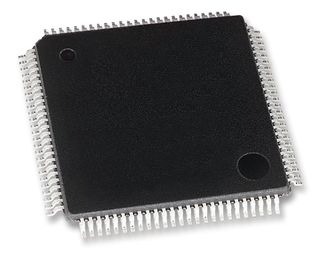
MCU 16-bit dSPIC33 dsPIC RISC 128KB Flash 3.3V 100-Pin TQFP Tray, DSPIC33FJ128GP310-I/PT, Microchip

dsPIC33F General Purpose Digital Signal Controller with seamless migration options to PIC24 MCUs and dsPIC30F DSC

  • Operating RangeDC – 40 MIPS (40 MIPS @ 3.0-3.6V)Industrial temperature range (-40°C to +85°C)High-Performance DSC CPUModified Harvard architectureC compiler optimized instruction set16-bit wide data path24-bit wide instructionsLinear program memory addressing up to 4M instruction wordsLinear data memory addressing up to 64 Kbytes83 base instructions: mostly 1 word/1 cycleSixteen 16-bit General Purpose RegistersTwo 40-bit accumulators: – With rounding and saturation optionsFlexible and powerful addressing modes: – Indirect, Modulo and Bit-ReversedSoftware stack16 x 16 fractional/integer multiply operations32/16 and 16/16 divide operationsSingle-cycle multiply and accumulate: – Accumulator write back for DSP operations – Dual data fetchUp to ±16-bit shifts for up to 40-bit dataDirect Memory Access (DMA)8-channel hardware DMA:2 Kbytes dual ported DMA buffer area (DMA RAM) to store data transferred via DMA: – Allows data transfer between RAM and a peripheral while CPU is executing code (no cycle stealing)Most peripherals support DMAInterrupt Controller5-cycle latency118 interrupt vectorsUp to 67 available interrupt sourcesUp to 5 external interrupts7 programmable priority levels5 processor exceptionsDigital I/OProgrammable digital I/O pinsWake-up/Interrupt-on-Change pinsOutput pins can drive from 3.0V to 3.6VAll digital input pins are 5V tolerant4 mA sink on all I/O pinsSystem ManagementFlexible clock options – External, crystal, resonator, internal RC – Fully integrated PLL – Extremely low jitter PLLPower-up TimerOscillator Start-up Timer/StabilizerWatchdog Timer with its own RC oscillatorFail-Safe Clock MonitorReset by multiple sourcesPower ManagementOn-chip 2.5V voltage regulatorSwitch between clock sources in real timeIdle, Sleep and Doze modes with fast wake-up Timers/Capture/Compare/PWMTimer/Counters, up to nine 16-bit timers: – Can pair up to make four 32-bit timers – 1 timer runs as Real-Time Clock with external 32.768 kHz oscillator – Programmable prescalerInput Capture (up to 8 channels): – Capture on up, down or both edges – 16-bit capture input functions – 4-deep FIFO on each captureOutput Compare (up to 8 channels): – Single or Dual 16-Bit Compare mode – 16-bit Glitchless PWM modeCommunication Modules3-wire SPI (up to 2 modules): – Framing supports I/O interface to simple codecs – Supports 8-bit and 16-bit data – Supports all serial clock formats and sampling modesI2C™ (up to 2 modules): – Full Multi-Master Slave mode support – 7-bit and 10-bit addressing – Bus collision detection and arbitration – Integrated signal conditioning – Slave address maskingUART (up to 2 modules): – Interrupt on address bit detect – Interrupt on UART error – Wake-up on Start bit from Sleep mode – 4-character TX and RX FIFO buffers – LIN bus support – IrDA® encoding and decoding in hardware – High-Speed Baud mode – Hardware Flow Control with CTS and RTSData Converter Interface (DCI) module: – Codec interface – Supports I2S and AC’97 protocols – Up to 16-bit data words, up to 16 words per frame – 4-word deep TX and RX buffersAnalog-to-Digital Converters (ADCs)Up to two ADC modules in a device10-bit, 1.1 Msps or 12-bit, 500 Ksps conversion: – 2, 4 or 8 simultaneous samples – Multiple input channels with auto-scanning – Conversion start can be manual or synchronized with 1 of 4 trigger sources – Conversion possible in Sleep mode – ±2 LSb max integral nonlinearity – ±1 LSb max differential nonlinearityCMOS Flash TechnologyLow-power, high-speed Flash technologyFully static design3.3V (±10%) operating voltageIndustrial temperatureLow-power consumptionPackaging:100-pin TQFP (14x14x1 mm and 12x12x1 mm)80-pin TQFP (12x12x1 mm)64-pin TQFP (10x10x1 mm)
  • Характеристики

    Schedule_b

    8542310000

    Operating_supply_voltage

    3.3 V

    Operating_temperature

    -40 to 85 °C

    Pin_count

    100

    Product_dimensions

    12 x 12 x 1 mm

    Specifications

    https://4donline.ihs.com/images/VipMasterIC/IC/MCHP/MCHPS03391/MCHPS03391-1.pdf?hkey=52A5661711E402568146F3353EA87419

    Max_speed

    40 MHz

    Number_of_timers

    9

    Бренд

    Country_of_origin

    Thailand

    Eccn

    3A991.A.2

    Htsn

    8542310001

    Тип интерфейса

    I2C/SPI/UART

    Number_of_programmable_i_os

    85

    Lead_finish

    Matte Tin

    Mounting

    Surface Mount

    SKU: DSPIC33FJ128GP310-I/PT

    Description

    dsPIC33F General Purpose Digital Signal Controller with seamless migration options to PIC24 MCUs and dsPIC30F DSC

  • Operating RangeDC – 40 MIPS (40 MIPS @ 3.0-3.6V)Industrial temperature range (-40°C to +85°C)High-Performance DSC CPUModified Harvard architectureC compiler optimized instruction set16-bit wide data path24-bit wide instructionsLinear program memory addressing up to 4M instruction wordsLinear data memory addressing up to 64 Kbytes83 base instructions: mostly 1 word/1 cycleSixteen 16-bit General Purpose RegistersTwo 40-bit accumulators: – With rounding and saturation optionsFlexible and powerful addressing modes: – Indirect, Modulo and Bit-ReversedSoftware stack16 x 16 fractional/integer multiply operations32/16 and 16/16 divide operationsSingle-cycle multiply and accumulate: – Accumulator write back for DSP operations – Dual data fetchUp to ±16-bit shifts for up to 40-bit dataDirect Memory Access (DMA)8-channel hardware DMA:2 Kbytes dual ported DMA buffer area (DMA RAM) to store data transferred via DMA: – Allows data transfer between RAM and a peripheral while CPU is executing code (no cycle stealing)Most peripherals support DMAInterrupt Controller5-cycle latency118 interrupt vectorsUp to 67 available interrupt sourcesUp to 5 external interrupts7 programmable priority levels5 processor exceptionsDigital I/OProgrammable digital I/O pinsWake-up/Interrupt-on-Change pinsOutput pins can drive from 3.0V to 3.6VAll digital input pins are 5V tolerant4 mA sink on all I/O pinsSystem ManagementFlexible clock options – External, crystal, resonator, internal RC – Fully integrated PLL – Extremely low jitter PLLPower-up TimerOscillator Start-up Timer/StabilizerWatchdog Timer with its own RC oscillatorFail-Safe Clock MonitorReset by multiple sourcesPower ManagementOn-chip 2.5V voltage regulatorSwitch between clock sources in real timeIdle, Sleep and Doze modes with fast wake-up Timers/Capture/Compare/PWMTimer/Counters, up to nine 16-bit timers: – Can pair up to make four 32-bit timers – 1 timer runs as Real-Time Clock with external 32.768 kHz oscillator – Programmable prescalerInput Capture (up to 8 channels): – Capture on up, down or both edges – 16-bit capture input functions – 4-deep FIFO on each captureOutput Compare (up to 8 channels): – Single or Dual 16-Bit Compare mode – 16-bit Glitchless PWM modeCommunication Modules3-wire SPI (up to 2 modules): – Framing supports I/O interface to simple codecs – Supports 8-bit and 16-bit data – Supports all serial clock formats and sampling modesI2C™ (up to 2 modules): – Full Multi-Master Slave mode support – 7-bit and 10-bit addressing – Bus collision detection and arbitration – Integrated signal conditioning – Slave address maskingUART (up to 2 modules): – Interrupt on address bit detect – Interrupt on UART error – Wake-up on Start bit from Sleep mode – 4-character TX and RX FIFO buffers – LIN bus support – IrDA® encoding and decoding in hardware – High-Speed Baud mode – Hardware Flow Control with CTS and RTSData Converter Interface (DCI) module: – Codec interface – Supports I2S and AC’97 protocols – Up to 16-bit data words, up to 16 words per frame – 4-word deep TX and RX buffersAnalog-to-Digital Converters (ADCs)Up to two ADC modules in a device10-bit, 1.1 Msps or 12-bit, 500 Ksps conversion: – 2, 4 or 8 simultaneous samples – Multiple input channels with auto-scanning – Conversion start can be manual or synchronized with 1 of 4 trigger sources – Conversion possible in Sleep mode – ±2 LSb max integral nonlinearity – ±1 LSb max differential nonlinearityCMOS Flash TechnologyLow-power, high-speed Flash technologyFully static design3.3V (±10%) operating voltageIndustrial temperatureLow-power consumptionPackaging:100-pin TQFP (14x14x1 mm and 12x12x1 mm)80-pin TQFP (12x12x1 mm)64-pin TQFP (10x10x1 mm)
  • Additional information

    Schedule_b

    8542310000

    Operating_supply_voltage

    3.3 V

    Operating_temperature

    -40 to 85 °C

    Pin_count

    100

    Product_dimensions

    12 x 12 x 1 mm

    Specifications

    https://4donline.ihs.com/images/VipMasterIC/IC/MCHP/MCHPS03391/MCHPS03391-1.pdf?hkey=52A5661711E402568146F3353EA87419

    Max_speed

    40 MHz

    Number_of_timers

    9

    Бренд

    Country_of_origin

    Thailand

    Eccn

    3A991.A.2

    Htsn

    8542310001

    Тип интерфейса

    I2C/SPI/UART

    Number_of_programmable_i_os

    85

    Lead_finish

    Matte Tin

    Mounting

    Surface Mount