Описание
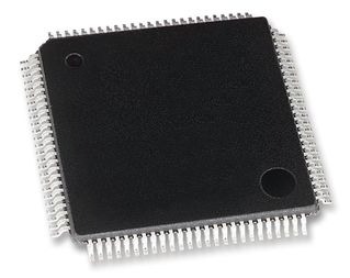
The TMS470R1A288 devices are members of the Texas Instruments TMS470R1x family of general-purpose 16/32-bit reduced instruction set computer (RISC) microcontrollers. The A288 microcontroller offers high performance utilizing the high-speed ARM7TDMI 16/32-bit RISC central processing unit (CPU), resulting in a high instruction throughput while maintaining greater code efficiency. The ARM7TDMI 16/32-bit RISC CPU views memory as a linear collection of bytes numbered upwards from zero. The A288 utilizes the big-endian format where the most significant byte of a word is stored at the lowest-numbered byte and the least significant byte at the highest numbered byte.High-end embedded control applications demand more performance from their controllers while maintaining low costs. The A288 RISC core architecture offers solutions to these performance and cost demands while maintaining low power consumption.The enhanced real-time interrupt (RTI) module on the A288 has the option to be driven by the oscillator clock. The digital watchdog (DWD) is a 25-bit resettable decrementing counter that provides a system reset when the watchdog counter expires. This data sheet includes device-specific information such as memory and peripheral select assignment, interrupt priority, and a device memory map.The A288 memory includes general-purpose SRAM supporting single-cycle read/write accesses in byte, half-word, and word modes.The flash memory on this device is a nonvolatile, electrically erasable and programmable memory implemented with a 32-bit-wide data bus interface. When in pipeline mode, the flash operates with a system clock frequency of up to 48 MHz. The flash operates with a system clock frequency of up to 24 MHz.The memory security module (MSM) and JTAG security module (JSM) prevent unauthorized access and visibility to on-chip memory, thereby preventing reverse engineering or manipulation of proprietary code.The A288 device has ten communication interfaces: two SPIs, two SCIs, two SCCs, a C2SI, and three I2Cs. The SPI provides a convenient method of serial interaction for high-speed communications between similar shift-register type devices. The SCI is a full-duplex, serial I/O interface intended for asynchronous communication between the CPU and other peripherals using the standard non-return-to-zero (NRZ) format. The SCC uses a serial, multimaster communication protocol that efficiently supports distributed real-time control with robust communication rates of up to 1 megabit per second (Mbps). The SCC is ideal for applications operating in noisy and harsh environments (e.g., industrial fields) that require reliable serial communication or multiplexed wiring. The C2SIb allows the A288 to transmit and receive messages on a class II network following an SAE J1850(2) standard. The I2C module is a multi-master communication module providing an interface between the A288 microcontroller and an I2C-compatible device via the I2C serial bus. The I2C supports both 100 Kbps and 400 Kbps speeds. For more detailed functional information on the SPI, SCI, and CAN peripherals.The HET is an advanced intelligent timer that provides sophisticated timing functions for real-time applications. The timer is software-controlled, using a reduced instruction set, with a specialized timer micro machine and an attached I/O port. The HET can be used for compare, capture, or general-purpose I/O. It is especially well suited for applications requiring multiple sensor information and drive actuators with complex and accurate time pulses. The HET used in this device is the high-end timer lite. It has fewer I/Os than the usual 32 in a standard HET.
- 24-MHz System Clock (48-MHz Pipeline)
- Independent 16/32-Bit Instruction Set
- Open Architecture With Third-Party Support
- Built-In Debug Module
- 288K-Byte Program Flash
- Two Banks With 8 Contiguous Sectors
- 16K-Byte Static RAM (SRAM)
- Memory Security Module (MSM)
- JTAG Security Module
- Low-Power Modes: STANDBY and HALT
- Extended Industrial Temperature Range
- 32-Bit Address Space Decoding
- Bus Supervision for Memory/Peripherals
- Digital Watchdog (DWD) Timer
- Analog Watchdog (AWD) Timer
- Enhanced Real-Time Interrupt (RTI)
- Interrupt Expansion Module (IEM)
- System Integrity and Failure Detection
- ICE Breaker
- 32 Control Packets and 16 Channels
- Multiply-by-8 Internal ZPLL Option
- ZPLL Bypass Mode
- 12 Programmable I/O Channels: 12 High-Resolution Pins
- High-Resolution Share Feature (XOR)
- High-End Timer RAM 64-Instruction Capacity
- Programmable Low-Frequency External Clock (CLK)
- Two Serial Peripheral Interfaces (SPIs)
- 255 Programmable Baud Rates
- Two Serial Communication Interfaces (SCIs)
- 224 Selectable Baud Rates
- Asynchronous/Isosynchronous Modes
- Class II Serial Interface B (C2SIb)
- Normal 10.4 Kbps and 4X Mode 41.6 Kbps
- Two Standard CAN Controllers (SCC)
- 16-Mailbox Capacity
- Fully Compliant With CAN Protocol, Version 2.0B
- Three Inter-Integrated Circuit (I2C) Modules
- Multi-Master and Slave Interfaces
- Up to 400 Kbps (Fast Mode)
- 7- and 10-Bit Address Capability
- 64-Word FIFO Buffer
- Single- or Continuous-Conversion Modes
- 1.55 µsMinimum Sample/Conversion Time
- Calibration Mode and Self-Test Features
- Supports 8- and 16-Bit Expansion Bus Memory Interface Mappings
- 42 I/O Expansion Bus Pins