MCU 16-bit/32-bit LPC2000 ARM7TDMI-S RISC 512KB Flash 3.3V 64-Pin LQFP Tray, LPC2138FBD64,151, NXP

The LPC2131/32/34/36/38 microcontrollers are based on a 16/32-bit ARM7TDMI-S CPU with real-time emulation and embedded trace support, that combine the microcontroller with 32 kB, 64 kB, 128 kB, 256 kB and 512 kB of embedded high-speed flash memory. A 128-bit wide memory interface and a unique accelerator architecture enable 32-bit code execution at maximum clock rate. For critical code size applications, the alternative 16-bit Thumb mode reduces code by more than 30 % with minimal performance penalty. Due to their tiny size and low power consumption, these microcontrollers are ideal for applications where miniaturization is a key requirement, such as access control and point-of-sale. With a wide range of serial communications interfaces and on-chip SRAM options of 8 kB, 16 kB, and 32 kB, they are very well suited for communication gateways and protocol converters, soft modems, voice recognition and low-end imaging, providing both large buffer size and high processing power. Various 32-bit timers, single or dual 10-bit 8-channel ADC(s), 10-bit DAC, PWM channels and 47 GPIO lines with up to nine edge or level sensitive external interrupt pins make these microcontrollers particularly suitable for industrial control and medical systems.

2.1 Enhancements brought by LPC213x/01 devices

  • Fast GPIO ports enable port pin toggling up to 3.5 times faster than the original LPC213x. They also allow for a port pin to be read at any time regardless of its function.
  • Dedicated result registers for ADC(s) reduce interrupt overhead.
  • UART0/1 include fractional baud rate generator, auto-bauding capabilities and handshake flow-control fully implemented in hardware.
  • Additional BOD control enables further reduction of power consumption.

2.2 Key features common for LPC213x and LPC213x/01

  • 16/32-bit ARM7TDMI-S microcontroller in a tiny LQFP64 or HVQFN64 package.
  • 8/16/32 kB of on-chip static RAM and 32/64/128/256/512 kB of on-chip flash program memory. 128-bit wide interface/accelerator enables high-speed 60 MHz operation.
  • In-System Programming/In-Application Programming (ISP/IAP) via on-chip bootloader software. Single flash sector or full chip erase in 400 ms and programming of 256 B in 1 ms.
  • EmbeddedICE RT and Embedded Trace interfaces offer real-time debugging with the on-chip RealMonitor software and high-speed tracing of instruction execution.
  • One (LPC2131/32) or two (LPC2134/36/38) 8-channel 10-bit ADCs provide a total of up to 16 analog inputs, with conversion times as low as 2.44 µs per channel.
  • Single 10-bit DAC provides variable analog output (LPC2132/34/36/38).
  • Two 32-bit timers/external event counters (with four capture and four compare channels each), PWM unit (six outputs) and watchdog.
  • Low power Real-time clock with independent power and dedicated 32 kHz clock input.
  • Multiple serial interfaces including two UARTs (16C550), two Fast I²C-bus (400 kbit/s), SPI and SSP with buffering and variable data length capabilities.
  • Vectored interrupt controller with configurable priorities and vector addresses.
  • Up to forty-seven 5 V tolerant general purpose I/O pins in tiny LQFP64 or HVQFN package.
  • Up to nine edge or level sensitive external interrupt pins available.
  • 60 MHz maximum CPU clock available from programmable on-chip PLL with settling time of 100 µs.
  • On-chip integrated oscillator operates with external crystal in range of 1 MHz to 30 MHz and with external oscillator up to 50 MHz.
  • Power saving modes include Idle and Power-down.
  • Individual enable/disable of peripheral functions as well as peripheral clock scaling down for additional power optimization.
  • Processor wake-up from Power-down mode via external interrupt or BOD.
  • Single power supply chip with POR and BOD circuits:
    • CPU operating voltage range of 3.0 V to 3.6 V (3.3 V ± 10 %) with 5 V tolerant I/O pads.
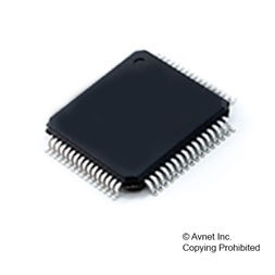
Характеристики

Program_memory_type

Flash

Supplier_package

LQFP

Specifications

https://4donline.ihs.com/images/VipMasterIC/IC/PHGL/PHGLS22279/PHGLS22279-1.pdf?hkey=52A5661711E402568146F3353EA87419

Schedule_b

8542310000

Ram_size

32 KB

Program_memory_size

512 Kb

Product_dimensions

10.1 x 10.1 x 1.4 mm

Pin_count

64

Operating_temperature

-40 to 85 °C

Operating_supply_voltage

3.3000 V

Watchdog

1

Eccn

EAR99

Instruction_set_architecture

RISC

Htsn

8542310001

Тип интерфейса

I2C/SPI/SSP

Device_core

ARM7TDMI-S

Data_bus_width

16, 32 Bit

Бренд

On_chip_adc

2(8-chx10-bit)

Min_operating_supply_voltage

3 V

Number_of_timers

2

Number_of_programmable_i_os

47

Mounting

Surface Mount

Max_speed

60 MHz

Max_processing_temp

260 °C

Max_power_dissipation

1500 mW

Max_operating_supply_voltage

3.6 V

Lead_finish

Matte Tin

Артикул: LPC2138FBD64,151

Описание

The LPC2131/32/34/36/38 microcontrollers are based on a 16/32-bit ARM7TDMI-S CPU with real-time emulation and embedded trace support, that combine the microcontroller with 32 kB, 64 kB, 128 kB, 256 kB and 512 kB of embedded high-speed flash memory. A 128-bit wide memory interface and a unique accelerator architecture enable 32-bit code execution at maximum clock rate. For critical code size applications, the alternative 16-bit Thumb mode reduces code by more than 30 % with minimal performance penalty. Due to their tiny size and low power consumption, these microcontrollers are ideal for applications where miniaturization is a key requirement, such as access control and point-of-sale. With a wide range of serial communications interfaces and on-chip SRAM options of 8 kB, 16 kB, and 32 kB, they are very well suited for communication gateways and protocol converters, soft modems, voice recognition and low-end imaging, providing both large buffer size and high processing power. Various 32-bit timers, single or dual 10-bit 8-channel ADC(s), 10-bit DAC, PWM channels and 47 GPIO lines with up to nine edge or level sensitive external interrupt pins make these microcontrollers particularly suitable for industrial control and medical systems.

2.1 Enhancements brought by LPC213x/01 devices

  • Fast GPIO ports enable port pin toggling up to 3.5 times faster than the original LPC213x. They also allow for a port pin to be read at any time regardless of its function.
  • Dedicated result registers for ADC(s) reduce interrupt overhead.
  • UART0/1 include fractional baud rate generator, auto-bauding capabilities and handshake flow-control fully implemented in hardware.
  • Additional BOD control enables further reduction of power consumption.

2.2 Key features common for LPC213x and LPC213x/01

  • 16/32-bit ARM7TDMI-S microcontroller in a tiny LQFP64 or HVQFN64 package.
  • 8/16/32 kB of on-chip static RAM and 32/64/128/256/512 kB of on-chip flash program memory. 128-bit wide interface/accelerator enables high-speed 60 MHz operation.
  • In-System Programming/In-Application Programming (ISP/IAP) via on-chip bootloader software. Single flash sector or full chip erase in 400 ms and programming of 256 B in 1 ms.
  • EmbeddedICE RT and Embedded Trace interfaces offer real-time debugging with the on-chip RealMonitor software and high-speed tracing of instruction execution.
  • One (LPC2131/32) or two (LPC2134/36/38) 8-channel 10-bit ADCs provide a total of up to 16 analog inputs, with conversion times as low as 2.44 µs per channel.
  • Single 10-bit DAC provides variable analog output (LPC2132/34/36/38).
  • Two 32-bit timers/external event counters (with four capture and four compare channels each), PWM unit (six outputs) and watchdog.
  • Low power Real-time clock with independent power and dedicated 32 kHz clock input.
  • Multiple serial interfaces including two UARTs (16C550), two Fast I²C-bus (400 kbit/s), SPI and SSP with buffering and variable data length capabilities.
  • Vectored interrupt controller with configurable priorities and vector addresses.
  • Up to forty-seven 5 V tolerant general purpose I/O pins in tiny LQFP64 or HVQFN package.
  • Up to nine edge or level sensitive external interrupt pins available.
  • 60 MHz maximum CPU clock available from programmable on-chip PLL with settling time of 100 µs.
  • On-chip integrated oscillator operates with external crystal in range of 1 MHz to 30 MHz and with external oscillator up to 50 MHz.
  • Power saving modes include Idle and Power-down.
  • Individual enable/disable of peripheral functions as well as peripheral clock scaling down for additional power optimization.
  • Processor wake-up from Power-down mode via external interrupt or BOD.
  • Single power supply chip with POR and BOD circuits:
    • CPU operating voltage range of 3.0 V to 3.6 V (3.3 V ± 10 %) with 5 V tolerant I/O pads.

Детали

Program_memory_type

Flash

Supplier_package

LQFP

Specifications

https://4donline.ihs.com/images/VipMasterIC/IC/PHGL/PHGLS22279/PHGLS22279-1.pdf?hkey=52A5661711E402568146F3353EA87419

Schedule_b

8542310000

Ram_size

32 KB

Program_memory_size

512 Kb

Product_dimensions

10.1 x 10.1 x 1.4 mm

Pin_count

64

Operating_temperature

-40 to 85 °C

Operating_supply_voltage

3.3000 V

Watchdog

1

Eccn

EAR99

Instruction_set_architecture

RISC

Htsn

8542310001

Тип интерфейса

I2C/SPI/SSP

Device_core

ARM7TDMI-S

Data_bus_width

16, 32 Bit

Бренд

On_chip_adc

2(8-chx10-bit)

Min_operating_supply_voltage

3 V

Number_of_timers

2

Number_of_programmable_i_os

47

Mounting

Surface Mount

Max_speed

60 MHz

Max_processing_temp

260 °C

Max_power_dissipation

1500 mW

Max_operating_supply_voltage

3.6 V

Lead_finish

Matte Tin