Описание
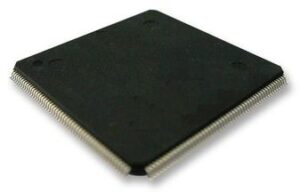
NXP Semiconductors designed the LPC2468 microcontroller around a 16-bit/32-bit ARM7TDMI-S CPU core with real-time debug interfaces that include both JTAG and embedded trace. The LPC2468 has 512 kB of on-chip high-speed flash memory. This flash memory includes a special 128-bit wide memory interface and accelerator architecture that enables the CPU to execute sequential instructions from flash memory at the maximum 72 MHz system clock rate. This feature is available only on the LPC2000 ARM microcontroller family of products. The LPC2468 can execute both 32-bit ARM and 16-bit Thumb instructions. Support for the two instruction sets means engineers can choose to optimize their application for either performance or code size at the sub-routine level. When the core executes instructions in Thumb state it can reduce code size by more than 30 % with only a small loss in performance while executing instructions in ARM state maximizes core performance.
- ARM7TDMI-S processor, running at up to 72 MHz
- 98 kB on-chip SRAM includes:
- 64 kB of SRAM on the ARM local bus for high performance CPU access.
- 16 kB SRAM for Ethernet interface
- Serial Interfaces
- Standard ARM test/debug interface for compatibility with existing tools.
- Emulation trace module supports real-time trace.
- Single 3.3 V power supply (3.0 V to 3.6 V).
- Four reduced power modes: idle, sleep, power-down, and deep power-down.
- Four external interrupt inputs configurable as edge/level sensitive. All pins on port 0 and port 2 can be used as edge sensitive interrupt sources.
- On-chip power-on reset.
- Boundary scan for simplified board testing.
- Versatile pin function selections allow more possibilities for using on-chip peripheral functions


