Описание
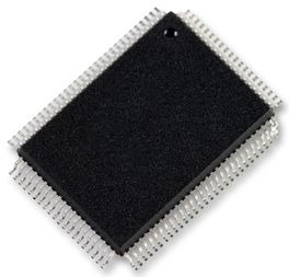
The H8S/2628 Group are single-chip microcomputers made up of the high-speed H8S/2600 CPU as its core, and the peripheral functions required to configure a system. The H8S/2600 CPU has an instruction set that is compatible with the H8/300 and H8/300H CPUs.This LSI is equipped with a data transfer controller (DTC), ROM and RAM memory, a PC break controller (PBC), a 16-bit timer pulse unit (TPU), a programmable pulse generator (PPG), a watchdog timer (WDT), a serial communication interface (SCI), a controller area network (HCAN), a synchronous serial communication unit (SSU), an A/D converter, and I/O ports as onchip peripheral modules required for system configuration. This LSI is suitable for use as an embedded microcomputer for high-level control systems. A single-power flash memory (FZTATTM) version is available for this LSI’s ROM. This provides flexibility as it can be reprogrammed in no time to cope with all situations from the early stages of mass production to full-scale mass production. This is particularly applicable to application devices with specifications that will most probably change.
- High-speed H8S/2600 central processing unit with an internal 16-bit architecture oUpward-compatible with H8/300 and H8/300H CPUs on an object level oSixteen 16-bit general registers o69 basic instructions
- Various peripheral functions oPC break controller oData transfer controller o16-bit timer-pulse unit (TPU) o8-bit timer (TMR) oProgrammable pulse generator (PPG) oWatchdog timer oAsynchronous or clocked synchronous serial communication interface (SCI) oController area network (HCAN) oSynchronous serial communication unit (SSU) o10-bit A/D converter oClock pulse generator
- On-chip memory oRAM: 8 kbytes oROM: 128 kbytes
- General I/O ports oI/O pins: 59 oInput-only pins: 17
- Supports various power-down states