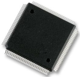
Freescale Automotiv MCUs, S912XEP100W1MALR, NXP

The MC9S12XE-Family of micro controllers is a further development of the S12XD-Family including new features for enhanced system integrity and greater functionality. These new features include a Memory Protection Unit (MPU) and Error Correction Code (ECC) on the Flash memory together with enhanced EEPROM functionality (EEE), an enhanced XGATE, an Internally filtered, frequency modulated Phase Locked Loop (IPLL) and an enhanced ATD. The MC9S12XE-Family delivers 32-bit performance with all the advantages and efficiencies of a 16 bit MCU. It retains the low cost, power consumption, EMC and code-size efficiency advantages currently enjoyed by users of Freescale’s existing 16-Bit MC9S12 and S12X MCU families. There is a high level of compatibility between the S12XE and S12XD families. The MC9S12XE-Family features an enhanced version of the performance-boosting XGATE co-processor which is programmable in “C” language and runs at twice the bus frequency of the S12X with an instruction set optimized for data movement, logic and bit manipulation instructions and which can service any peripheral module on the device. The new enhanced version has improved interrupt handling capability and is fully compatible with the existing XGATE module. The MC9S12XE-Family is composed of standard on-chip peripherals including up to 64Kbytes of RAM, eight asynchronous serial communications interfaces (SCI), three serial peripheral interfaces (SPI), an 8- channel IC/OC enhanced capture timer (ECT), two 16-channel, 12-bit analog-to-digital converters, an 8- channel pulse-width modulator (PWM), five CAN 2.0 A, B software compatible modules (MSCAN12), two inter-IC bus blocks (IIC), an 8-channel 24-bit periodic interrupt timer (PIT) and an 8-channel 16-bit standard timer module (TIM). In addition to the I/O ports available in each module, up to 26 further I/O ports are available with interrupt capability allowing Wake-Up from STOP or WAIT modes. The MC9S12XE-Family is available in 208- Pin MAPBGA, 144-Pin LQFP, 112-Pin LQFP or 80-Pin QFP options.

  • 16-Bit CPU12X
    • Upward compatible with MC9S12 instruction set with the exception of five Fuzzy instructions (MEM, WAV, WAVR, REV, REVW) which have been removed
    • Enhanced indexed addressing
    • Access to large data segments independent of PPAGE
  • INT (interrupt module)
  • EBI (external bus interface)(available in 208-Pin and 144-Pin packages only)
    • Up to four chip select outputs to select 16K, 1M, 2M and up to 4MByte address spaces
    • Each chip select output can be configured to complete transaction on either the time-out of one of the two wait state generators or the deassertion of EWAIT signal
  • MMC (module mapping control)
  • DBG (debug module)
    • Monitoring of CPU and/or XGATE busses with tag-type or force-type breakpoint requests
    • 64 x 64-bit circular trace buffer captures change-of-flow or memory access information
  • XGATE
  • OSC_LCP (oscillator)
  • IPLL (Internally filtered, frequency modulated phase-locked-loop clock generation)
  • CRG (clock and reset generation)
    • COP watchdog
    • Real time interrupt
    • Clock monitor
    • Fast wake up from STOP in self clock mode
  • Memory Options
    • 128K, 256k, 384K, 512K, 768K and 1M byte Flash
    • 2K, 4K byte emulated EEPROM
    • 12K, 16K, 24K, 32K, 48K and 64K Byte RAM
  • Flash General Features
    • 64 data bits plus 8 syndrome ECC (Error Correction Code) bits allow single bit failure correction and double fault detection
    • Erase sector size 1024 bytes
    • Automated program and erase algorithm
  • Low-power wake-up timer (API)
    • Available in all modes including Full Stop Mode
    • Trimmable to +-5% accuracy
    • Time-out periods range from 0.2ms to ~13s with a 0.2ms resolution
  • Input/Output
    • Up to 152 general-purpose input/output (I/O) pins plus 2 input-only pins
    • Hysteresis and configurable pull up/pull down device on all input pins
    • Configurable drive strength on all output pins
  • Package Options
    • 208-pin MAPBGA
    • 144-pin low-profile quad flat-pack (LQFP)
    • 112-pin low-profile quad flat-pack (LQFP)
    • 80-pin quad flat-pack (QFP)
  • 50MHz maximum CPU bus frequency, 100MHz maximum XGATE bus frequency
Характеристики

Schedule_b

8542390000

Operating_supply_voltage

3.3, 5 V

Operating_temperature

-40 to 125 °C

Packaging

Tape and Reel

Program_memory_size

1 MB

Program_memory_type

Flash

Ram_size

8 KB

Screening_level

Automotive

On_chip_adc

2(16-chx12-bit)

Special_features

CAN Controller

Specifications

http://cache.freescale.com/files/microcontrollers/doc/data_sheet/MC9S12XEP100RMV1.pdf

Watchdog

1

Max_speed

50 MHz

Number_of_timers

1

Бренд

Instruction_set_architecture

CISC

Country_of_origin

Malaysia

Data_bus_width

16 Bit

Data_memory_size

4 Kb

Device_core

S12X

Eccn

3A991.A.2

Family

S912XEP100

Htsn

8542310001

Тип интерфейса

CAN/I2C/SCI/SPI

Number_of_programmable_i_os

91

Max_expanded_memory_size

4 MB

Max_operating_supply_voltage

5.5 V

Min_operating_supply_voltage

3.13 V

Mounting

Surface Mount

Msl_level

3

Артикул: S912XEP100W1MALR

Описание

The MC9S12XE-Family of micro controllers is a further development of the S12XD-Family including new features for enhanced system integrity and greater functionality. These new features include a Memory Protection Unit (MPU) and Error Correction Code (ECC) on the Flash memory together with enhanced EEPROM functionality (EEE), an enhanced XGATE, an Internally filtered, frequency modulated Phase Locked Loop (IPLL) and an enhanced ATD. The MC9S12XE-Family delivers 32-bit performance with all the advantages and efficiencies of a 16 bit MCU. It retains the low cost, power consumption, EMC and code-size efficiency advantages currently enjoyed by users of Freescale’s existing 16-Bit MC9S12 and S12X MCU families. There is a high level of compatibility between the S12XE and S12XD families. The MC9S12XE-Family features an enhanced version of the performance-boosting XGATE co-processor which is programmable in “C” language and runs at twice the bus frequency of the S12X with an instruction set optimized for data movement, logic and bit manipulation instructions and which can service any peripheral module on the device. The new enhanced version has improved interrupt handling capability and is fully compatible with the existing XGATE module. The MC9S12XE-Family is composed of standard on-chip peripherals including up to 64Kbytes of RAM, eight asynchronous serial communications interfaces (SCI), three serial peripheral interfaces (SPI), an 8- channel IC/OC enhanced capture timer (ECT), two 16-channel, 12-bit analog-to-digital converters, an 8- channel pulse-width modulator (PWM), five CAN 2.0 A, B software compatible modules (MSCAN12), two inter-IC bus blocks (IIC), an 8-channel 24-bit periodic interrupt timer (PIT) and an 8-channel 16-bit standard timer module (TIM). In addition to the I/O ports available in each module, up to 26 further I/O ports are available with interrupt capability allowing Wake-Up from STOP or WAIT modes. The MC9S12XE-Family is available in 208- Pin MAPBGA, 144-Pin LQFP, 112-Pin LQFP or 80-Pin QFP options.

  • 16-Bit CPU12X
    • Upward compatible with MC9S12 instruction set with the exception of five Fuzzy instructions (MEM, WAV, WAVR, REV, REVW) which have been removed
    • Enhanced indexed addressing
    • Access to large data segments independent of PPAGE
  • INT (interrupt module)
  • EBI (external bus interface)(available in 208-Pin and 144-Pin packages only)
    • Up to four chip select outputs to select 16K, 1M, 2M and up to 4MByte address spaces
    • Each chip select output can be configured to complete transaction on either the time-out of one of the two wait state generators or the deassertion of EWAIT signal
  • MMC (module mapping control)
  • DBG (debug module)
    • Monitoring of CPU and/or XGATE busses with tag-type or force-type breakpoint requests
    • 64 x 64-bit circular trace buffer captures change-of-flow or memory access information
  • XGATE
  • OSC_LCP (oscillator)
  • IPLL (Internally filtered, frequency modulated phase-locked-loop clock generation)
  • CRG (clock and reset generation)
    • COP watchdog
    • Real time interrupt
    • Clock monitor
    • Fast wake up from STOP in self clock mode
  • Memory Options
    • 128K, 256k, 384K, 512K, 768K and 1M byte Flash
    • 2K, 4K byte emulated EEPROM
    • 12K, 16K, 24K, 32K, 48K and 64K Byte RAM
  • Flash General Features
    • 64 data bits plus 8 syndrome ECC (Error Correction Code) bits allow single bit failure correction and double fault detection
    • Erase sector size 1024 bytes
    • Automated program and erase algorithm
  • Low-power wake-up timer (API)
    • Available in all modes including Full Stop Mode
    • Trimmable to +-5% accuracy
    • Time-out periods range from 0.2ms to ~13s with a 0.2ms resolution
  • Input/Output
    • Up to 152 general-purpose input/output (I/O) pins plus 2 input-only pins
    • Hysteresis and configurable pull up/pull down device on all input pins
    • Configurable drive strength on all output pins
  • Package Options
    • 208-pin MAPBGA
    • 144-pin low-profile quad flat-pack (LQFP)
    • 112-pin low-profile quad flat-pack (LQFP)
    • 80-pin quad flat-pack (QFP)
  • 50MHz maximum CPU bus frequency, 100MHz maximum XGATE bus frequency

Детали

Schedule_b

8542390000

Operating_supply_voltage

3.3, 5 V

Operating_temperature

-40 to 125 °C

Packaging

Tape and Reel

Program_memory_size

1 MB

Program_memory_type

Flash

Ram_size

8 KB

Screening_level

Automotive

On_chip_adc

2(16-chx12-bit)

Special_features

CAN Controller

Specifications

http://cache.freescale.com/files/microcontrollers/doc/data_sheet/MC9S12XEP100RMV1.pdf

Watchdog

1

Max_speed

50 MHz

Number_of_timers

1

Бренд

Instruction_set_architecture

CISC

Country_of_origin

Malaysia

Data_bus_width

16 Bit

Data_memory_size

4 Kb

Device_core

S12X

Eccn

3A991.A.2

Family

S912XEP100

Htsn

8542310001

Тип интерфейса

CAN/I2C/SCI/SPI

Number_of_programmable_i_os

91

Max_expanded_memory_size

4 MB

Max_operating_supply_voltage

5.5 V

Min_operating_supply_voltage

3.13 V

Mounting

Surface Mount

Msl_level

3