EXTENDED TEMPERATURE SERIAL INTERFACE CODECFILTER COMBO FAMILY, TP3054WM-X, Texas Instruments

The TP3054, TP3057 family consists of µ-law and A-law monolithic PCM CODEC/filters utilizing the A/D and D/A conversion architecture shown in , and a serial PCM interface. The devices are fabricated using TI"s advanced double-poly CMOS process (microCMOS).The encode portion of each device consists of an input gain adjust amplifier, an active RC pre-filter which eliminates very high frequency noise prior to entering a switched-capacitor band-pass filter that rejects signals below 200 Hz and above 3400 Hz. Also included are auto-zero circuitry and a companding coder which samples the filtered signal and encodes it in the companded µ-law or A-law PCM format. The decode portion of each device consists of an expanding decoder, which reconstructs the analog signal from the companded µ-law or A-law code, a low-pass filter which corrects for the sin x/x response of the decoder output and rejects signals above 3400 Hz followed by a single-ended power amplifier capable of driving low impedance loads. The devices require two 1.536 MHz, 1.544 MHz or 2.048 MHz transmit and receive master clocks, which may be asynchronous; transmit and receive bit clocks, which may vary from 64 kHz to 2.048 MHz; and transmit and receive frame sync pulses. The timing of the frame sync pulses and PCM data is compatible with both industry standard formats. 

  • -40°C to +85°C Operation
  • Complete CODEC and Filtering System (COMBO) Including:
    • Transmit High-Pass and Low-Pass Filtering
    • Receive Low-Pass Filter with Sin x/x Correction
    • Active RC Noise Filters
    • µ-Law or A-Law Compatible COder and DECoder
    • Internal Precision Voltage Reference
    • Serial I/O Interface
    • Internal Auto-Zero Circuitry
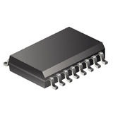
  • µ-Law, 16-Pin – TP3054
  • A-Law, 16-Pin – TP3057
  • Designed for D3/D4 and CCITT Spplications
  • ±5V Operation
  • Low Operating Power – Typically 50 mW
  • Power-Down Standby Mode – Typically 3 mW
  • Automatic Power-Down
  • TTL or CMOS Compatible Digital Interfaces
  • Maximizes Line Interface Card Circuit Density
  • Dual-In-Line or PCC Surface Mount Packages
  • See also AN-370, “Techniques for Designing with CODEC/Filter COMBO Circuits” (SNLA136)
  • Характеристики

    Бренд

    Operating_supply_voltage

    ±5 V

    Number_of_adc_inputs

    1

    Supplier_package

    SOIC W

    Specifications

    http://www.ti.com/general/docs/lit/getliterature.tsp?genericPartNumber=TP3057-X&&fileType=pdf

    Schedule_b

    8472909002

    Product_dimensions

    10.5 x 7.6 x 2.35 mm

    Pin_count

    16

    Operating_temperature

    -55 to 125 °C

    Number_of_dac_outputs

    1

    Number_of_adcs

    1

    Количество каналов

    1ADC /2 DAC

    Msl_level

    4

    Mounting

    Surface Mount

    Max_processing_temp

    260, 300

    Lead_finish

    Tin/Lead

    Kind

    PCM

    Htsn

    8542390001

    Eccn

    5A991.B

    Country_of_origin

    United States

    SKU: TP3054WM-X

    Description

    The TP3054, TP3057 family consists of µ-law and A-law monolithic PCM CODEC/filters utilizing the A/D and D/A conversion architecture shown in , and a serial PCM interface. The devices are fabricated using TI"s advanced double-poly CMOS process (microCMOS).The encode portion of each device consists of an input gain adjust amplifier, an active RC pre-filter which eliminates very high frequency noise prior to entering a switched-capacitor band-pass filter that rejects signals below 200 Hz and above 3400 Hz. Also included are auto-zero circuitry and a companding coder which samples the filtered signal and encodes it in the companded µ-law or A-law PCM format. The decode portion of each device consists of an expanding decoder, which reconstructs the analog signal from the companded µ-law or A-law code, a low-pass filter which corrects for the sin x/x response of the decoder output and rejects signals above 3400 Hz followed by a single-ended power amplifier capable of driving low impedance loads. The devices require two 1.536 MHz, 1.544 MHz or 2.048 MHz transmit and receive master clocks, which may be asynchronous; transmit and receive bit clocks, which may vary from 64 kHz to 2.048 MHz; and transmit and receive frame sync pulses. The timing of the frame sync pulses and PCM data is compatible with both industry standard formats. 

  • -40°C to +85°C Operation
  • Complete CODEC and Filtering System (COMBO) Including:
    • Transmit High-Pass and Low-Pass Filtering
    • Receive Low-Pass Filter with Sin x/x Correction
    • Active RC Noise Filters
    • µ-Law or A-Law Compatible COder and DECoder
    • Internal Precision Voltage Reference
    • Serial I/O Interface
    • Internal Auto-Zero Circuitry
  • µ-Law, 16-Pin – TP3054
  • A-Law, 16-Pin – TP3057
  • Designed for D3/D4 and CCITT Spplications
  • ±5V Operation
  • Low Operating Power – Typically 50 mW
  • Power-Down Standby Mode – Typically 3 mW
  • Automatic Power-Down
  • TTL or CMOS Compatible Digital Interfaces
  • Maximizes Line Interface Card Circuit Density
  • Dual-In-Line or PCC Surface Mount Packages
  • See also AN-370, “Techniques for Designing with CODEC/Filter COMBO Circuits” (SNLA136)
  • Additional information

    Бренд

    Operating_supply_voltage

    ±5 V

    Number_of_adc_inputs

    1

    Supplier_package

    SOIC W

    Specifications

    http://www.ti.com/general/docs/lit/getliterature.tsp?genericPartNumber=TP3057-X&&fileType=pdf

    Schedule_b

    8472909002

    Product_dimensions

    10.5 x 7.6 x 2.35 mm

    Pin_count

    16

    Operating_temperature

    -55 to 125 °C

    Number_of_dac_outputs

    1

    Number_of_adcs

    1

    Количество каналов

    1ADC /2 DAC

    Msl_level

    4

    Mounting

    Surface Mount

    Max_processing_temp

    260, 300

    Lead_finish

    Tin/Lead

    Kind

    PCM

    Htsn

    8542390001

    Eccn

    5A991.B

    Country_of_origin

    United States