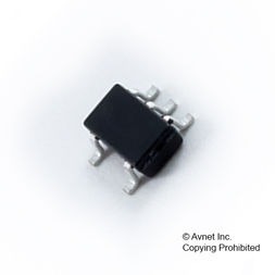
Analog Switch Single SPST 5-Pin TSOP, 74LVC1G66GV-Q100,1, Nexperia

The 74LVC1G66-Q100 provides one single pole, single-throw analog switch function. It has two input/output terminals (Y and Z) and an active HIGH enable input pin (E). When E is LOW, the analog switch is turned off. Schmitt trigger action at the enable input makes the circuit tolerant of slower input rise and fall times across the entire VCC range from 1.65 V to 5.5 V. This product has been qualified to the Automotive Electronics Council (AEC) standard Q100 (Grade 1) and is suitable for use in automotive applications.

  • Automotive product qualification in accordance with AEC-Q100 (Grade 1)
    • Specified from -40 °C to +85 °C and from -40 °C to +125 °C
  • Wide supply voltage range from 1.65 V to 5.5 V
  • Very low ON resistance:
    • 7.5 O (typical) at VCC = 2.7 V
    • 6.5 O (typical) at VCC = 3.3 V
    • 6 O (typical) at VCC = 5 V
  • Switch current capability of 32 mA
  • High noise immunity
  • CMOS low power consumption
  • TTL interface compatibility at 3.3 V
  • Latch-up performance meets requirements of JESD78 Class I
  • ESD protection:
    • MIL-STD-883, method 3015 exceeds 2000 V
    • HBM JESD22-A114F exceeds 2000 V
    • MM JESD22-A115-A exceeds 200 V (C = 200 pF, R = 0 O)
  • Enable input accepts voltages up to 5.5 V
  • Multiple package options

Характеристики

Бренд

Country_of_origin

Malaysia

Msl_level

1

Mounting

Surface Mount

Max_turn_on_time

5.3@1.95V ns

Max_propagation_delay_btb

0.2@5.5, 0.3@3.6, 0.4@2.7, 0.8@1.95 ns

Max_processing_temp

260

Max_power_dissipation

250 mW

Max_on_resistance

195@1.95V Ohm

Max_low_lev_output_current

50 mA

Max_high_lev_output_current

50 mA

Lead_finish

Tin

Kind

Analog Switch

Input_signal_type

Single

Htsn

8542390001

Eccn

EAR99

Конфигурация

Single SPST

Operating_temp

-40 to 125 °C

Chip_enable_signals

Yes

Number_of_inputs_per_chip

1

Operating_supply_voltage

1.65 V, 5.5

Operating_supply_current

0.2@5.5V

Max_on_resistance_range

150 to 250 Ohm

Supplier_package

TSOP

Number_of_outputs_per_chip

1

Specifications

http://www.nxp.com/documents/data_sheet/74LVC1G66_Q100.pdf

Schedule_b

8542390000

Product_dimensions

3.1 x 1.7 x 1 mm

Power_supply_type

Single

Polarity

Non-Inverting

Pin_count

5

Output_signal_type

Single-Ended

Number_of_channels_per_chip

1

Артикул: 74LVC1G66GV-Q100,1

Описание

The 74LVC1G66-Q100 provides one single pole, single-throw analog switch function. It has two input/output terminals (Y and Z) and an active HIGH enable input pin (E). When E is LOW, the analog switch is turned off. Schmitt trigger action at the enable input makes the circuit tolerant of slower input rise and fall times across the entire VCC range from 1.65 V to 5.5 V. This product has been qualified to the Automotive Electronics Council (AEC) standard Q100 (Grade 1) and is suitable for use in automotive applications.

  • Automotive product qualification in accordance with AEC-Q100 (Grade 1)
    • Specified from -40 °C to +85 °C and from -40 °C to +125 °C
  • Wide supply voltage range from 1.65 V to 5.5 V
  • Very low ON resistance:
    • 7.5 O (typical) at VCC = 2.7 V
    • 6.5 O (typical) at VCC = 3.3 V
    • 6 O (typical) at VCC = 5 V
  • Switch current capability of 32 mA
  • High noise immunity
  • CMOS low power consumption
  • TTL interface compatibility at 3.3 V
  • Latch-up performance meets requirements of JESD78 Class I
  • ESD protection:
    • MIL-STD-883, method 3015 exceeds 2000 V
    • HBM JESD22-A114F exceeds 2000 V
    • MM JESD22-A115-A exceeds 200 V (C = 200 pF, R = 0 O)
  • Enable input accepts voltages up to 5.5 V
  • Multiple package options

Детали

Бренд

Country_of_origin

Malaysia

Msl_level

1

Mounting

Surface Mount

Max_turn_on_time

5.3@1.95V ns

Max_propagation_delay_btb

0.2@5.5, 0.3@3.6, 0.4@2.7, 0.8@1.95 ns

Max_processing_temp

260

Max_power_dissipation

250 mW

Max_on_resistance

195@1.95V Ohm

Max_low_lev_output_current

50 mA

Max_high_lev_output_current

50 mA

Lead_finish

Tin

Kind

Analog Switch

Input_signal_type

Single

Htsn

8542390001

Eccn

EAR99

Конфигурация

Single SPST

Operating_temp

-40 to 125 °C

Chip_enable_signals

Yes

Number_of_inputs_per_chip

1

Operating_supply_voltage

1.65 V, 5.5

Operating_supply_current

0.2@5.5V

Max_on_resistance_range

150 to 250 Ohm

Supplier_package

TSOP

Number_of_outputs_per_chip

1

Specifications

http://www.nxp.com/documents/data_sheet/74LVC1G66_Q100.pdf

Schedule_b

8542390000

Product_dimensions

3.1 x 1.7 x 1 mm

Power_supply_type

Single

Polarity

Non-Inverting

Pin_count

5

Output_signal_type

Single-Ended

Number_of_channels_per_chip

1