Analog Switch Single DPDT 16-Pin UQFN T/R, TS3USB3200RSVR, Texas Instruments

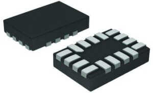
The TS3USB3200 is a double-pole, double throw (DPDT) multiplexer that includes a high speed Mobile High-Definition Link (MHL) or Mobility Display Port (MyDP) switch and a USB 2.0 High-Speed (480Mbps) switch in the same package. Additionally included is a single-pole, double throw (SPDT) USB/MHL or MyDP ID switch for easy information control. These configurations allow the system designer to use a common USB or Mico-USB connector for both MHL/MyDP video signals and USB data. The TS3USB3200 has a VCC range of 2.7V to 4.3V and also has the option to be powered by VBUS without VCC. The device supports a over-voltage tolerance (OVT) feature which allows the I/O pins to withstand over-voltage conditions (up to 5.5V). The power-off protection feature forces all I/O pins to be in high impedance mode when power is not present. This allows full isolation of the signals lines without excessive leakage current. The select pins of TS3USB3200 are compatible with 1.8V control voltage, allowing them to be directly interfaced with the General Purpose I/O (GPIO) from a mobile processor.The TS3USB3200 comes with a small 16-pin QFN package (2.6mm x 1.8mm in size), which makes it a perfect candidate for mobile applications. 

  • VCC Range: 2.7V to 4.3V
  • Mobile High-definition Link (MHL) or Mobility Display Port (MyDP) Switch
    • Bandwidth (–3dB): 5.5 GHz
    • Ron (Typ): 5.7O
    • Con (Typ): 2.5pF
  • USB Switch
    • Bandwidth (–3dB): 5.5 GHz
    • Ron (Typ): 4.6O
    • Con (Typ): 2.5pF
  • Current Consumption: 40µA Typ
  • Special Features
    • Flexible Power Control: Device can be Powered by VBUS Without VCC or by VCC Alone
    • IOFF Protection Prevents Current Leakage in Powered Down State (VCC and VBUS= 0 V)
    • 1.8-V Compatible Control Inputs (SEL1, SEL2, and PSEL)
    • Over-Voltage Tolerance (OVT) on all I/O Pins up to 5.5V Without External Components
  • ESD Performance:
    • 3.5kV Human Body Model (A114B, Class II)
    • 1kV Charged Device Model (C101)
  • Package:
    • 16-pin QFN Package (2.6 x 1.8 mm, 0.4 mm Pitch)
  • Характеристики

    Бренд

    Operating_temp

    -40 to 85 °C

    Output_signal_type

    Differential

    Pin_count

    16

    Polarity

    Non-Inverting

    Power_supply_type

    Dual

    Product_dimensions

    1.8 x 2.6 x 0.55 mm

    Propagat_delay_test_condit

    5 pF

    Schedule_b

    8542390000

    Specifications

    http://www.ti.com/general/docs/lit/getliterature.tsp?genericPartNumber=TS3USB3200&&fileType=pdf

    Number_of_outputs_per_chip

    4

    Supplier_package

    UQFN

    Max_on_resistance_range

    5 to 10 Ohm

    Operating_supply_current

    0.07@4.3V

    Operating_supply_voltage

    2.7, 3, 4.3, 5 V, 5.5

    Number_of_inputs_per_chip

    2

    Max_data_rate

    480 Mbps

    Chip_enable_signals

    Yes

    Конфигурация

    Single DPDT

    Country_of_origin

    Thailand

    Eccn

    EAR99

    Htsn

    8542390001

    Input_signal_type

    Differential

    Kind

    Analog Switch

    Lead_finish

    Gold

    Max_frequency_25_deg_c_vcc

    6000@3.3 MHz

    Max_on_resistance

    6.5@2.7V Ohm

    Max_processing_temp

    260

    Max_propagation_delay_btb

    0.1@3.3 ns

    Max_turn_on_time

    400@4.3V ns

    Mounting

    Surface Mount

    Msl_level

    1

    Number_of_channels_per_chip

    1

    Артикул: TS3USB3200RSVR

    Описание

    The TS3USB3200 is a double-pole, double throw (DPDT) multiplexer that includes a high speed Mobile High-Definition Link (MHL) or Mobility Display Port (MyDP) switch and a USB 2.0 High-Speed (480Mbps) switch in the same package. Additionally included is a single-pole, double throw (SPDT) USB/MHL or MyDP ID switch for easy information control. These configurations allow the system designer to use a common USB or Mico-USB connector for both MHL/MyDP video signals and USB data. The TS3USB3200 has a VCC range of 2.7V to 4.3V and also has the option to be powered by VBUS without VCC. The device supports a over-voltage tolerance (OVT) feature which allows the I/O pins to withstand over-voltage conditions (up to 5.5V). The power-off protection feature forces all I/O pins to be in high impedance mode when power is not present. This allows full isolation of the signals lines without excessive leakage current. The select pins of TS3USB3200 are compatible with 1.8V control voltage, allowing them to be directly interfaced with the General Purpose I/O (GPIO) from a mobile processor.The TS3USB3200 comes with a small 16-pin QFN package (2.6mm x 1.8mm in size), which makes it a perfect candidate for mobile applications. 

  • VCC Range: 2.7V to 4.3V
  • Mobile High-definition Link (MHL) or Mobility Display Port (MyDP) Switch
    • Bandwidth (–3dB): 5.5 GHz
    • Ron (Typ): 5.7O
    • Con (Typ): 2.5pF
  • USB Switch
    • Bandwidth (–3dB): 5.5 GHz
    • Ron (Typ): 4.6O
    • Con (Typ): 2.5pF
  • Current Consumption: 40µA Typ
  • Special Features
    • Flexible Power Control: Device can be Powered by VBUS Without VCC or by VCC Alone
    • IOFF Protection Prevents Current Leakage in Powered Down State (VCC and VBUS= 0 V)
    • 1.8-V Compatible Control Inputs (SEL1, SEL2, and PSEL)
    • Over-Voltage Tolerance (OVT) on all I/O Pins up to 5.5V Without External Components
  • ESD Performance:
    • 3.5kV Human Body Model (A114B, Class II)
    • 1kV Charged Device Model (C101)
  • Package:
    • 16-pin QFN Package (2.6 x 1.8 mm, 0.4 mm Pitch)
  • Детали

    Бренд

    Operating_temp

    -40 to 85 °C

    Output_signal_type

    Differential

    Pin_count

    16

    Polarity

    Non-Inverting

    Power_supply_type

    Dual

    Product_dimensions

    1.8 x 2.6 x 0.55 mm

    Propagat_delay_test_condit

    5 pF

    Schedule_b

    8542390000

    Specifications

    http://www.ti.com/general/docs/lit/getliterature.tsp?genericPartNumber=TS3USB3200&&fileType=pdf

    Number_of_outputs_per_chip

    4

    Supplier_package

    UQFN

    Max_on_resistance_range

    5 to 10 Ohm

    Operating_supply_current

    0.07@4.3V

    Operating_supply_voltage

    2.7, 3, 4.3, 5 V, 5.5

    Number_of_inputs_per_chip

    2

    Max_data_rate

    480 Mbps

    Chip_enable_signals

    Yes

    Конфигурация

    Single DPDT

    Country_of_origin

    Thailand

    Eccn

    EAR99

    Htsn

    8542390001

    Input_signal_type

    Differential

    Kind

    Analog Switch

    Lead_finish

    Gold

    Max_frequency_25_deg_c_vcc

    6000@3.3 MHz

    Max_on_resistance

    6.5@2.7V Ohm

    Max_processing_temp

    260

    Max_propagation_delay_btb

    0.1@3.3 ns

    Max_turn_on_time

    400@4.3V ns

    Mounting

    Surface Mount

    Msl_level

    1

    Number_of_channels_per_chip

    1