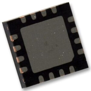
Analog Switch Single 4PDT 16-Pin HXQFN-U EP T/R, NX3DV2567HR-Q100X, NXP

The NX3DV2567-Q100 is a four-pole double-throw analog switch (4PDT) optimized for switching WLAN-SIM supply, data and control signals. It has one digital select input (S) and four switches each with two independent input/outputs (nY0 and nY1) and a common input/output (nZ). Schmitt-trigger action at S, makes the circuit tolerant to slower input rise and fall times across the entire VCC range from 1.4 V to 4.3 V. Lower-level logic signals can drive pin S without a significant increase in supply current ICC, due to a low input voltage threshold. This characteristic makes it possible for the NX3DV2567-Q100 to switch 4.3 V signals with a 1.8 V digital controller, eliminating the need for logic level translation. The NX3DV2567-Q100 allows signals with amplitude up to VCC to be transmitted from nZ to nY0 or nY1; or from nY0 or nY1 to nZ. This product has been qualified to the Automotive Electronics Council (AEC) standard Q100 (Grade 1) and is suitable for use in automotive applications.

  • Automotive product qualification in accordance with AEC-Q100 (Grade 1)
    • Specified from -40 °C to +85 °C and from -40 °C to +125 °C
  • Wide supply voltage range from 1.4 V to 4.3 V
  • Very low ON resistance for supply path:
    • 0.5 O (typical) at VCC = 1.8 V
    • 0.45 O (typical) at VCC = 2.7 V
  • Low ON resistance for data path:
    • 7 O (typical) at VCC = 1.8 V
    • 6 O (typical) at VCC = 2.7 V
  • Low ON capacitance for data path
  • Wide -3 dB bandwidth > 160 MHz
  • Break-before-make switching
  • High noise immunity
  • ESD protection:
    • MIL-STD-883, method 3015 Class 3A exceeds 4000 V
    • HBM JESD22-A114F Class 3A exceeds 4000 V
    • MIL-STD-883, method 3015 Class 3A I/O to GND exceeds 7000 V
    • HBM JESD22-A114F Class 3A I/O to GND exceeds 7000 V
    • CDM AEC-Q100-011 revision B exceeds 1000 V
  • CMOS low-power consumption
  • Latch-up performance exceeds 100 mA per JESD 78B Class II Level A
  • 1.8 V control logic at VCC = 3.6 V
  • Control input accepts voltages above supply voltage
  • Very low supply current, even when input is below VCC
  • High current handling capability (350 mA continuous current under 3.3 V supply forsupply path switch)
Характеристики

Бренд

Screening_level

Automotive

Operating_temp

-40 to 125 °C

Output_signal_type

Differential

Pin_count

16

Polarity

Non-Inverting

Power_supply_type

Single

Product_dimensions

3 x 3 x 0.45(Max)

Schedule_b

8542390000

Specifications

http://www.nxp.com/documents/data_sheet/NX3DV2567_Q100.pdf

Number_of_outputs_per_chip

2

Supplier_package

HXQFN-U EP

Operating_supply_current

0.00015@4.3V mA

Operating_supply_voltage

1.4 V, 4.3

Number_of_inputs_per_chip

4

Chip_enable_signals

Yes

Конфигурация

Single 4PDT

Country_of_origin

Thailand

Eccn

EAR99

Htsn

8542390001

Input_signal_type

Differential

Kind

Analog Switch

Lead_finish

Gold Over Nickel Palladium

Max_frequency_25_deg_c_vcc

330@3.6 MHz

Max_high_lev_output_current

500 mA

Max_low_lev_output_current

500 mA

Max_on_resistance

11@1.8V Ohm

Max_power_dissipation

250 mW

Max_processing_temp

260

Max_turn_on_time

90@1.6V ns

Mounting

Surface Mount

Msl_level

3

Number_of_channels_per_chip

1

Артикул: NX3DV2567HR-Q100X

Описание

The NX3DV2567-Q100 is a four-pole double-throw analog switch (4PDT) optimized for switching WLAN-SIM supply, data and control signals. It has one digital select input (S) and four switches each with two independent input/outputs (nY0 and nY1) and a common input/output (nZ). Schmitt-trigger action at S, makes the circuit tolerant to slower input rise and fall times across the entire VCC range from 1.4 V to 4.3 V. Lower-level logic signals can drive pin S without a significant increase in supply current ICC, due to a low input voltage threshold. This characteristic makes it possible for the NX3DV2567-Q100 to switch 4.3 V signals with a 1.8 V digital controller, eliminating the need for logic level translation. The NX3DV2567-Q100 allows signals with amplitude up to VCC to be transmitted from nZ to nY0 or nY1; or from nY0 or nY1 to nZ. This product has been qualified to the Automotive Electronics Council (AEC) standard Q100 (Grade 1) and is suitable for use in automotive applications.

  • Automotive product qualification in accordance with AEC-Q100 (Grade 1)
    • Specified from -40 °C to +85 °C and from -40 °C to +125 °C
  • Wide supply voltage range from 1.4 V to 4.3 V
  • Very low ON resistance for supply path:
    • 0.5 O (typical) at VCC = 1.8 V
    • 0.45 O (typical) at VCC = 2.7 V
  • Low ON resistance for data path:
    • 7 O (typical) at VCC = 1.8 V
    • 6 O (typical) at VCC = 2.7 V
  • Low ON capacitance for data path
  • Wide -3 dB bandwidth > 160 MHz
  • Break-before-make switching
  • High noise immunity
  • ESD protection:
    • MIL-STD-883, method 3015 Class 3A exceeds 4000 V
    • HBM JESD22-A114F Class 3A exceeds 4000 V
    • MIL-STD-883, method 3015 Class 3A I/O to GND exceeds 7000 V
    • HBM JESD22-A114F Class 3A I/O to GND exceeds 7000 V
    • CDM AEC-Q100-011 revision B exceeds 1000 V
  • CMOS low-power consumption
  • Latch-up performance exceeds 100 mA per JESD 78B Class II Level A
  • 1.8 V control logic at VCC = 3.6 V
  • Control input accepts voltages above supply voltage
  • Very low supply current, even when input is below VCC
  • High current handling capability (350 mA continuous current under 3.3 V supply forsupply path switch)
Детали

Бренд

Screening_level

Automotive

Operating_temp

-40 to 125 °C

Output_signal_type

Differential

Pin_count

16

Polarity

Non-Inverting

Power_supply_type

Single

Product_dimensions

3 x 3 x 0.45(Max)

Schedule_b

8542390000

Specifications

http://www.nxp.com/documents/data_sheet/NX3DV2567_Q100.pdf

Number_of_outputs_per_chip

2

Supplier_package

HXQFN-U EP

Operating_supply_current

0.00015@4.3V mA

Operating_supply_voltage

1.4 V, 4.3

Number_of_inputs_per_chip

4

Chip_enable_signals

Yes

Конфигурация

Single 4PDT

Country_of_origin

Thailand

Eccn

EAR99

Htsn

8542390001

Input_signal_type

Differential

Kind

Analog Switch

Lead_finish

Gold Over Nickel Palladium

Max_frequency_25_deg_c_vcc

330@3.6 MHz

Max_high_lev_output_current

500 mA

Max_low_lev_output_current

500 mA

Max_on_resistance

11@1.8V Ohm

Max_power_dissipation

250 mW

Max_processing_temp

260

Max_turn_on_time

90@1.6V ns

Mounting

Surface Mount

Msl_level

3

Number_of_channels_per_chip

1