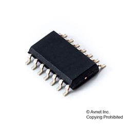
Analog Switch Quad SPST 14-Pin SOP T/R, HCF4066M013TR, STMicroelectronics

The HCF4066B is a monolithic integrated circuit fabricated in Metal Oxide Semiconductor technology available in DIP and SOP packages.The HCF4066B is a QUAD BILATERAL SWITCH intended for the transmission or multiplexing of analog or digital signals.It is pin for pin compatible with HCF4016B, but exhibits a much lower ON resistance. In addition, the ON resistance is relatively constant over the full input signal range. The HCF4066B consists of four independent bilateral switches. A single control signal is required per switch. Both the pand n device in a given switch are biased ON or OFF simultaneously by the control signal. As shown in schematic diagram, the well of the n-channel device on each switch is either tied to the input when the switch is ON or to VSS when the switch is OFF. This configuration eliminates the variation of the switch-transistor threshold voltage with input signal, and thus keeps the ON resistance low over the full operating signal range. The advantages over single channel switches include peak input signal voltage swings equal to the full supply voltage, and more constant ON impedance over the input signal range. For sample and hold applications, however, the HCF4016B is recommended.

  • 15V DIGITAL OR ± 7.5V PEAK TO PEAK SWITCHING
  • 125? TYPICAL ON RESISTANCE FOR 15V OPERATION
  • SWITCH ON RESISTANCE MATCHED TO WITHIN 5? TYP. OVER 15V SIGNAL INPUT RANGE
  • ON RESISTANCE FLAT OVER FULL PEAK TO PEAK SIGNAL RANGE
  • HIGH ON/OFF OUTPUT VOLTAGE RATIO: 65dB TYP. at fIS = 10KHz, RL = 10K?
  • HIGH DEGREE OF LINEARITY: < 0.5% DISTORTION TYP. at fIS = 1KHz, VIS =5VPP, VDD - VSS > 10V, RL = 10K?
  • EXTREMELY LOW OFF SWITCH LEAKAGE RESULTING IN VERY LOW OFFSET CURRENT AND HIGH EFFECTIVE OFF RESISTANCE: 10pA TYP. at VDD – VSS = 10V, Tamb = 25°C
  • EXTREMELY HIGH CONTROL INPUT IMPEDANCE (control circuit isolated from signal circuit 1012? typ.)
  • LOW CROSSTALK BETWEEN SWITCHES: 50dB Typ. at fIS = 0.9MHz, RL = 1K?
  • MATCHED CONTROL – INPUT TO SIGNAL OUTPUT CAPACITANCE: REDUCES OUTPUT SIGNAL TRANSIENTS
  • FREQUENCY RESPONSE SWITCH ON: 40MHz (Typ.)
  • QUIESCENT CURRENT SPECIF. UP TO 20V
  • 5V, 10V AND 15V PARAMETRIC RATINGS

Характеристики

Бренд

Конфигурация

Quad SPST

Msl_level

1

Mounting

Surface Mount

Max_turn_on_time

70@5V ns

Max_propagation_delay_btb

40 ns

Max_processing_temp

260

Max_power_dissipation

200 mW

Max_on_resistance

1050@5V Ohm

Lead_finish

Tin

Kind

Analog Switch

Input_signal_type

Single

Htsn

8542390001

Eccn

EAR99

Chip_enable_signals

Yes

Operating_temp

-55 to 125 °C

Number_of_inputs_per_chip

4

Operating_supply_voltage

20, 3 V

Max_on_resistance_range

>=1000 Ohm

Supplier_package

SOP

Number_of_outputs_per_chip

4

Specifications

https://4donline.ihs.com/images/VipMasterIC/IC/SGST/SGST-S-A0008386644/SGST-S-A0008386644-1.pdf?hkey=52A5661711E402568146F3353EA87419

Schedule_b

8542390000

Propagat_delay_test_condit

50 pF

Product_dimensions

8.75 x 4 x 1.65 mm

Power_supply_type

Single

Polarity

Non-Inverting

Pin_count

14

Output_signal_type

Single-Ended

Number_of_channels_per_chip

4

Артикул: HCF4066M013TR

Описание

The HCF4066B is a monolithic integrated circuit fabricated in Metal Oxide Semiconductor technology available in DIP and SOP packages.The HCF4066B is a QUAD BILATERAL SWITCH intended for the transmission or multiplexing of analog or digital signals.It is pin for pin compatible with HCF4016B, but exhibits a much lower ON resistance. In addition, the ON resistance is relatively constant over the full input signal range. The HCF4066B consists of four independent bilateral switches. A single control signal is required per switch. Both the pand n device in a given switch are biased ON or OFF simultaneously by the control signal. As shown in schematic diagram, the well of the n-channel device on each switch is either tied to the input when the switch is ON or to VSS when the switch is OFF. This configuration eliminates the variation of the switch-transistor threshold voltage with input signal, and thus keeps the ON resistance low over the full operating signal range. The advantages over single channel switches include peak input signal voltage swings equal to the full supply voltage, and more constant ON impedance over the input signal range. For sample and hold applications, however, the HCF4016B is recommended.

  • 15V DIGITAL OR ± 7.5V PEAK TO PEAK SWITCHING
  • 125? TYPICAL ON RESISTANCE FOR 15V OPERATION
  • SWITCH ON RESISTANCE MATCHED TO WITHIN 5? TYP. OVER 15V SIGNAL INPUT RANGE
  • ON RESISTANCE FLAT OVER FULL PEAK TO PEAK SIGNAL RANGE
  • HIGH ON/OFF OUTPUT VOLTAGE RATIO: 65dB TYP. at fIS = 10KHz, RL = 10K?
  • HIGH DEGREE OF LINEARITY: < 0.5% DISTORTION TYP. at fIS = 1KHz, VIS =5VPP, VDD - VSS > 10V, RL = 10K?
  • EXTREMELY LOW OFF SWITCH LEAKAGE RESULTING IN VERY LOW OFFSET CURRENT AND HIGH EFFECTIVE OFF RESISTANCE: 10pA TYP. at VDD – VSS = 10V, Tamb = 25°C
  • EXTREMELY HIGH CONTROL INPUT IMPEDANCE (control circuit isolated from signal circuit 1012? typ.)
  • LOW CROSSTALK BETWEEN SWITCHES: 50dB Typ. at fIS = 0.9MHz, RL = 1K?
  • MATCHED CONTROL – INPUT TO SIGNAL OUTPUT CAPACITANCE: REDUCES OUTPUT SIGNAL TRANSIENTS
  • FREQUENCY RESPONSE SWITCH ON: 40MHz (Typ.)
  • QUIESCENT CURRENT SPECIF. UP TO 20V
  • 5V, 10V AND 15V PARAMETRIC RATINGS

Детали

Бренд

Конфигурация

Quad SPST

Msl_level

1

Mounting

Surface Mount

Max_turn_on_time

70@5V ns

Max_propagation_delay_btb

40 ns

Max_processing_temp

260

Max_power_dissipation

200 mW

Max_on_resistance

1050@5V Ohm

Lead_finish

Tin

Kind

Analog Switch

Input_signal_type

Single

Htsn

8542390001

Eccn

EAR99

Chip_enable_signals

Yes

Operating_temp

-55 to 125 °C

Number_of_inputs_per_chip

4

Operating_supply_voltage

20, 3 V

Max_on_resistance_range

>=1000 Ohm

Supplier_package

SOP

Number_of_outputs_per_chip

4

Specifications

https://4donline.ihs.com/images/VipMasterIC/IC/SGST/SGST-S-A0008386644/SGST-S-A0008386644-1.pdf?hkey=52A5661711E402568146F3353EA87419

Schedule_b

8542390000

Propagat_delay_test_condit

50 pF

Product_dimensions

8.75 x 4 x 1.65 mm

Power_supply_type

Single

Polarity

Non-Inverting

Pin_count

14

Output_signal_type

Single-Ended

Number_of_channels_per_chip

4