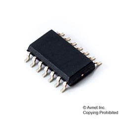
Analog Switch Quad SPST 14-Pin SOP T/R, CD4016BNSR, Texas Instruments

CD4016B Series types are quad bilateral switches intended for the transmission or multiplexing of analog or digital signals. Each of the four independent bilateral switches has a single control signal input which simultaneously biases both the p and n device in a given switch on or off. The CD4016 “B” Series types are supplied in 14-lead hermetic dual-in-line ceramic packages (F3A suffix),14-lead dual-in-line plastic packages (E suffix), 14-lead small-outline packages (M, MT, M96, and NSR suffixes),and 14-lead thin shrink small-outline packages (PW and PWR suffixes).

  • 20-V digital or ± 10-V peak-to-peak switching
  • 280-O typical on-state resistance for 15-V operation
  • Switch on-state resistance matched to within 10 O typ. over 15-V signal-input range
  • High on/off output-voltage ratio:
       65 dB typ. @ fis = 10 kHz, RL = 10 kO
  • High degree of linearity:
       <0.5% distortion typ. @ fis = 1 kHz, Vis = 5 Vp-p, VDD–VSS O
  • Extremely low off-state switch leakage resulting in very low offset current and high effective off-state resistance:
       100pA typ. @ VDD–VSS = 18 V, TA = 25°C
  • Extremely high control input impedance (control circuit isolated form signal circuit:
       1012Otyp.
  • Low crosstalk between switches:
       –50 dB typ. @ fis= 0.9 MHz, RL = 1 kO
  • Matched control-input to signal-output capacitance:
       Reduces output signal transients
  • Frequency response, switch on = 40MHz (typ.)
  • 100% tested for quiescent current at 20 V
  • Maximum control input current of 1 µA at 18 V over full package temperature range; 100 nA at 18 V and 25°C
  • 5-V, 10-V, and 15-V parametric ratings
  • Applications:
    • Analog signal switching/multiplexing
      • Signal gating
      • Squelch control
      • Chopper
      • Modulator
      • Demodulator
      • Commutating switch
    • Digital signal switching/multiplexing
    • CMOS logic implementation
    • Analog-to-digital & digital-to-analog conversion
    • Digital control of frequency, impedance, phase, and analog-signal gain
  • Характеристики

    Бренд

    Chip_enable_signals

    Yes

    Output_signal_type

    Single-Ended

    Pin_count

    14

    Power_supply_type

    Dual, Single

    Product_dimensions

    10.3 x 5.3 x 1.95 mm

    Propagat_delay_test_condit

    50 pF

    Schedule_b

    8542390000

    Specifications

    http://www.ti.com/general/docs/lit/getliterature.tsp?genericPartNumber=CD4016B-MIL&&fileType=pdf

    Number_of_outputs_per_chip

    4

    Supplier_package

    SOP

    Max_on_resistance_range

    >=1000 Ohm

    Operating_supply_voltage

    ±1.5, ±3, ±5 V, ±9, 18, 3

    Number_of_inputs_per_chip

    4

    Operating_temp

    -55 to 125 °C

    Country_of_origin

    United States

    Конфигурация

    Quad SPST

    Eccn

    EAR99

    Htsn

    8542390001

    Input_signal_type

    Single

    Kind

    Analog Switch

    Lead_finish

    Gold

    Max_on_resistance

    2000@10V Ohm

    Max_power_dissipation

    500 mW

    Max_processing_temp

    260

    Max_propagation_delay_btb

    100@5V, 30@15V ns, 40@10V

    Max_turn_on_time

    70@5V ns

    Mounting

    Surface Mount

    Msl_level

    1

    Number_of_channels_per_chip

    4

    Артикул: CD4016BNSR

    Описание

    CD4016B Series types are quad bilateral switches intended for the transmission or multiplexing of analog or digital signals. Each of the four independent bilateral switches has a single control signal input which simultaneously biases both the p and n device in a given switch on or off. The CD4016 “B” Series types are supplied in 14-lead hermetic dual-in-line ceramic packages (F3A suffix),14-lead dual-in-line plastic packages (E suffix), 14-lead small-outline packages (M, MT, M96, and NSR suffixes),and 14-lead thin shrink small-outline packages (PW and PWR suffixes).

  • 20-V digital or ± 10-V peak-to-peak switching
  • 280-O typical on-state resistance for 15-V operation
  • Switch on-state resistance matched to within 10 O typ. over 15-V signal-input range
  • High on/off output-voltage ratio:
       65 dB typ. @ fis = 10 kHz, RL = 10 kO
  • High degree of linearity:
       <0.5% distortion typ. @ fis = 1 kHz, Vis = 5 Vp-p, VDD–VSS O
  • Extremely low off-state switch leakage resulting in very low offset current and high effective off-state resistance:
       100pA typ. @ VDD–VSS = 18 V, TA = 25°C
  • Extremely high control input impedance (control circuit isolated form signal circuit:
       1012Otyp.
  • Low crosstalk between switches:
       –50 dB typ. @ fis= 0.9 MHz, RL = 1 kO
  • Matched control-input to signal-output capacitance:
       Reduces output signal transients
  • Frequency response, switch on = 40MHz (typ.)
  • 100% tested for quiescent current at 20 V
  • Maximum control input current of 1 µA at 18 V over full package temperature range; 100 nA at 18 V and 25°C
  • 5-V, 10-V, and 15-V parametric ratings
  • Applications:
    • Analog signal switching/multiplexing
      • Signal gating
      • Squelch control
      • Chopper
      • Modulator
      • Demodulator
      • Commutating switch
    • Digital signal switching/multiplexing
    • CMOS logic implementation
    • Analog-to-digital & digital-to-analog conversion
    • Digital control of frequency, impedance, phase, and analog-signal gain
  • Детали

    Бренд

    Chip_enable_signals

    Yes

    Output_signal_type

    Single-Ended

    Pin_count

    14

    Power_supply_type

    Dual, Single

    Product_dimensions

    10.3 x 5.3 x 1.95 mm

    Propagat_delay_test_condit

    50 pF

    Schedule_b

    8542390000

    Specifications

    http://www.ti.com/general/docs/lit/getliterature.tsp?genericPartNumber=CD4016B-MIL&&fileType=pdf

    Number_of_outputs_per_chip

    4

    Supplier_package

    SOP

    Max_on_resistance_range

    >=1000 Ohm

    Operating_supply_voltage

    ±1.5, ±3, ±5 V, ±9, 18, 3

    Number_of_inputs_per_chip

    4

    Operating_temp

    -55 to 125 °C

    Country_of_origin

    United States

    Конфигурация

    Quad SPST

    Eccn

    EAR99

    Htsn

    8542390001

    Input_signal_type

    Single

    Kind

    Analog Switch

    Lead_finish

    Gold

    Max_on_resistance

    2000@10V Ohm

    Max_power_dissipation

    500 mW

    Max_processing_temp

    260

    Max_propagation_delay_btb

    100@5V, 30@15V ns, 40@10V

    Max_turn_on_time

    70@5V ns

    Mounting

    Surface Mount

    Msl_level

    1

    Number_of_channels_per_chip

    4