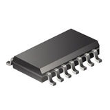
Analog Switch Quad SPST 14-Pin SOIC T/R, MC14016BDR2, ON Semiconductor

The MC14016B quad bilateral switch is constructed with MOS P-channel and N-channel enhancement mode devices in a single monolithic structure. Each MC14016B consists of four independent switches capable of controlling either digital or analog signals. The quad bilateral switch is used in signal gating, chopper, modulator, demodulator and CMOS logic implementation.

  • Diode Protection on All Inputs
  • Supply Voltage Range = 3.0 Vdc to 18 Vdc
  • Linearized Transfer Characteristics
  • Low Noise – 12 nV/sq. root (Cycle), f >= 1.0 kHz typical
  • Pin-for-Pin Replacements for CD4016B, CD4066B (Note improvedtransfer characteristic design causes more parasitic coupling capacitance than CD4016)
  • For Lower RON , Use The HC4016 High-Speed CMOS Device or The MC14066B
  • This Device Has Inputs and Outputs Which Do Not Have ESD Protection. Antistatic Precautions Must Be Taken.
  • Pb-Free Packages are Available*

Характеристики

Бренд

Chip_enable_signals

Yes

Msl_level

1

Mounting

Surface Mount

Max_propagation_delay_btb

12@15V ns, 15@10V, 45@5V

Max_processing_temp

260

Max_on_resistance

660@5V Ohm

Max_low_lev_output_current

25 mA

Lead_finish

Tin/Lead

Kind

Analog Switch

Htsn

8542390001

Eccn

EAR99

Country_of_origin

United States

Конфигурация

Quad SPST

Number_of_inputs_per_chip

4

Operating_temp

-55 to 125 °C

Operating_supply_voltage

18, 3 V

Max_on_resistance_range

400 to 1000 Ohm

Supplier_package

SOIC

Number_of_outputs_per_chip

4

Specifications

https://4donline.ihs.com/images/VipMasterIC/IC/ONSM/ONSMS20412/ONSMS20412-1.pdf?hkey=52A5661711E402568146F3353EA87419

Schedule_b

8542390000

Propagat_delay_test_condit

50 pF

Product_dimensions

8.75 x 4 x 1.5 mm

Power_supply_type

Single

Polarity

Non-Inverting

Pin_count

14

Output_signal_type

Single-Ended

Number_of_channels_per_chip

4

Артикул: MC14016BDR2

Описание

The MC14016B quad bilateral switch is constructed with MOS P-channel and N-channel enhancement mode devices in a single monolithic structure. Each MC14016B consists of four independent switches capable of controlling either digital or analog signals. The quad bilateral switch is used in signal gating, chopper, modulator, demodulator and CMOS logic implementation.

  • Diode Protection on All Inputs
  • Supply Voltage Range = 3.0 Vdc to 18 Vdc
  • Linearized Transfer Characteristics
  • Low Noise – 12 nV/sq. root (Cycle), f >= 1.0 kHz typical
  • Pin-for-Pin Replacements for CD4016B, CD4066B (Note improvedtransfer characteristic design causes more parasitic coupling capacitance than CD4016)
  • For Lower RON , Use The HC4016 High-Speed CMOS Device or The MC14066B
  • This Device Has Inputs and Outputs Which Do Not Have ESD Protection. Antistatic Precautions Must Be Taken.
  • Pb-Free Packages are Available*

Детали

Бренд

Chip_enable_signals

Yes

Msl_level

1

Mounting

Surface Mount

Max_propagation_delay_btb

12@15V ns, 15@10V, 45@5V

Max_processing_temp

260

Max_on_resistance

660@5V Ohm

Max_low_lev_output_current

25 mA

Lead_finish

Tin/Lead

Kind

Analog Switch

Htsn

8542390001

Eccn

EAR99

Country_of_origin

United States

Конфигурация

Quad SPST

Number_of_inputs_per_chip

4

Operating_temp

-55 to 125 °C

Operating_supply_voltage

18, 3 V

Max_on_resistance_range

400 to 1000 Ohm

Supplier_package

SOIC

Number_of_outputs_per_chip

4

Specifications

https://4donline.ihs.com/images/VipMasterIC/IC/ONSM/ONSMS20412/ONSMS20412-1.pdf?hkey=52A5661711E402568146F3353EA87419

Schedule_b

8542390000

Propagat_delay_test_condit

50 pF

Product_dimensions

8.75 x 4 x 1.5 mm

Power_supply_type

Single

Polarity

Non-Inverting

Pin_count

14

Output_signal_type

Single-Ended

Number_of_channels_per_chip

4