Analog Switch Quad SPST 14-Pin PDIP Bulk, HEF4016BP,652, Nexperia

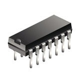
The HEF4016B has four independent analogue switches (transmission gates). Each switch has two input/output terminals (Y/Z) and an active HIGH enable input (E). When E is connected to VDD a low impedance bidirectional path between Y and Z is established (ON condition). When E is connected to VSS the switch is disabled and a high impedance between Y and Z is established (OFF condition). Current through a switch will not cause additional VDD current provided the voltage at the terminals of the switch is maintained within the supply voltage range; VDD = (VY , VZ ) = VSS

  • Fully static operation
  • 5 V, 10 V, and 15 V parametric ratings
  • Wide operating temperature range -40 ? to +85 ?
  • Complies with JEDEC standard JESD 13-B
Характеристики

Бренд

Конфигурация

Quad SPST

Mounting

Through Hole

Max_turn_on_time

80@5V ns

Max_propagation_delay_btb

10@15V ns, 20@10V, 50@5V

Max_processing_temp

260

Max_power_dissipation

400 mW

Max_on_resistance

690@5V Ohm

Lead_finish

Gold

Kind

Analog Switch

Input_signal_type

Single

Htsn

8542390001

Eccn

EAR99

Country_of_origin

United States

Chip_enable_signals

Yes

Operating_temp

-40 to 85 °C

Number_of_inputs_per_chip

4

Operating_supply_voltage

15.5, 4.5 V

Max_on_resistance_range

400 to 1000 Ohm

Supplier_package

PDIP

Number_of_outputs_per_chip

4

Specifications

https://assets.nexperia.com/documents/data-sheet/HEF4016B.pdf

Schedule_b

8542390000

Propagat_delay_test_condit

50 pF

Product_dimensions

19.5 x 6.48 x 3.2 mm

Power_supply_type

Single

Pin_count

14

Output_signal_type

Single-Ended

Number_of_channels_per_chip

4

Артикул: HEF4016BP,652

Описание

The HEF4016B has four independent analogue switches (transmission gates). Each switch has two input/output terminals (Y/Z) and an active HIGH enable input (E). When E is connected to VDD a low impedance bidirectional path between Y and Z is established (ON condition). When E is connected to VSS the switch is disabled and a high impedance between Y and Z is established (OFF condition). Current through a switch will not cause additional VDD current provided the voltage at the terminals of the switch is maintained within the supply voltage range; VDD = (VY , VZ ) = VSS

  • Fully static operation
  • 5 V, 10 V, and 15 V parametric ratings
  • Wide operating temperature range -40 ? to +85 ?
  • Complies with JEDEC standard JESD 13-B
Детали

Бренд

Конфигурация

Quad SPST

Mounting

Through Hole

Max_turn_on_time

80@5V ns

Max_propagation_delay_btb

10@15V ns, 20@10V, 50@5V

Max_processing_temp

260

Max_power_dissipation

400 mW

Max_on_resistance

690@5V Ohm

Lead_finish

Gold

Kind

Analog Switch

Input_signal_type

Single

Htsn

8542390001

Eccn

EAR99

Country_of_origin

United States

Chip_enable_signals

Yes

Operating_temp

-40 to 85 °C

Number_of_inputs_per_chip

4

Operating_supply_voltage

15.5, 4.5 V

Max_on_resistance_range

400 to 1000 Ohm

Supplier_package

PDIP

Number_of_outputs_per_chip

4

Specifications

https://assets.nexperia.com/documents/data-sheet/HEF4016B.pdf

Schedule_b

8542390000

Propagat_delay_test_condit

50 pF

Product_dimensions

19.5 x 6.48 x 3.2 mm

Power_supply_type

Single

Pin_count

14

Output_signal_type

Single-Ended

Number_of_channels_per_chip

4