Описание
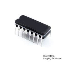
The redesigned analog switches now feature low on-resistance matching between switches (3O max) and guaranteed on-resistance flatness over the signal range (4O max). These low on-resistance switches conduct equally well in either direction. They guarantee low charge injection, low power consumption, and an ESD tolerance of 2000V minimum per Method 3015.7. The new design offers lower off-leakage current over temperature (less than 5nA at +85°C). They are quad, single-pole/single-throw (SPST) analog switches. This part is normally open (NO). Switching times are less than 150ns max for tON and less than 100ns max for tOFF. These devices operate from a single +10V to +30V supply, or bipolar ±4.5V to ±20V supplies. They are fabricated with a 44V silicon gate process.
- Plug-In Upgrade for Industry-Standard
- Improved RDS(ON) Match Between Channels (3O max)
- Guaranteed RFLAT(ON) Over Signal Range (4O)
- Improved Charge Injection (10pC max)
- Improved Off-Leakage Current Over Temperature (< 5nA at +85°C)
- Withstand Electrostatic Discharge (2000V min) per Method 3015.7
- Low RDS(ON) (35O max)
- Single-Supply Operation +10V to +30V
- Bipolar-Supply Operation ±4.5V to ±20V
- Low Power Consumption (35µW max)
- Rail-to-Rail Signal Handling
- TTL/CMOS-Logic Compatible
- -55°C to +125°C Temperature
- 16-pin CERDIP Package


