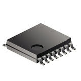
Analog Multiplexer Triple 2:1 16-Pin TSSOP T/R, CD4053BPWRG3, Texas Instruments

The CD405xB analog multiplexers and demuliplexers are digitally-controlled analog switches having low ON impedance and very low OFF leakage current. These multiplexer circuits dissipate extremely low quiescent power over the full VDD – VSS and VDD – VEE supply-voltage ranges, independent of the logic state of the control signals.

  • Wide Range of Digital and Analog Signal Levels
    • Digital: 3 V to 20 V
    • Analog: =20 VP-P
  • Low ON Resistance,125 O (Typical) Over 15 VP-P
    Signal Input Range for VDD – VEE = 18 V
  • High OFF Resistance, Channel Leakage of ±100
    pA (Typical) at VDD – VEE = 18 V
  • Logic-Level Conversion for Digital Addressing
    Signals of 3 V to 20 V (VDD – VSS = 3 V to 20 V)
    to Switch Analog Signals to 20 VP-P (VDD – VEE =
    20 V) Matched Switch Characteristics, rON = 5 O
    (Typical) for VDD – VEE = 15 V Very Low Quiescent
    Power Dissipation Under All Digital-Control Input
    and Supply Conditions, 0.2 µW (Typical) at VDD
    VSS = VDD – VEE = 10 V
  • Binary Address Decoding on Chip
  • 5 V, 10 V, and 15 V Parametric Ratings
  • 100% Tested for Quiescent Current at 20 V
  • Maximum Input Current of 1 µA at 18 V Over Full
    Package Temperature Range, 100 nA at 18 V and
    25°C
  • Break-Before-Make Switching Eliminates Channel
    Overlap
  • Характеристики

    Бренд

    Chip_enable_signals

    Yes

    Max_on_resistance

    1050@5V Ohm

    Number_of_channels_per_chip

    3

    Number_of_outputs_per_chip

    3

    Max_turn_on_time

    720@5V ns

    Output_signal_type

    Single-Ended

    Power_supply_type

    Dual, Single

    Max_propagation_delay_btb

    20@15V ns, 30@10V, 60@5V

    Propagat_delay_test_condit

    50 pF

    Max_on_resist_range

    >=1000 Ohm

    Number_of_inputs_per_chip

    6

    Msl_level

    1

    Конфигурация

    Triple 2:1

    Country_of_origin

    United States

    Eccn

    EAR99

    Htsn

    8542390001

    Input_signal_type

    Single

    Kind

    Analog Multiplexer

    Lead_finish

    Tin

    Max_processing_temp

    260

    Mounting

    Surface Mount

    Operat_supply_voltage

    ±2.5, ±3, ±5 V, ±9, 20, 3

    Operat_temperature

    -55 to 125 °C

    Pin_count

    16

    Product_dimensions

    5.1 x 4.5 x 1.05 mm

    Schedule_b

    8542390000

    Specifications

    http://www.ti.com/general/docs/lit/getliterature.tsp?genericPartNumber=CD4051B-MIL&&fileType=pdf

    Supplier_package

    TSSOP

    Артикул: CD4053BPWRG3

    Описание

    The CD405xB analog multiplexers and demuliplexers are digitally-controlled analog switches having low ON impedance and very low OFF leakage current. These multiplexer circuits dissipate extremely low quiescent power over the full VDD – VSS and VDD – VEE supply-voltage ranges, independent of the logic state of the control signals.

  • Wide Range of Digital and Analog Signal Levels
    • Digital: 3 V to 20 V
    • Analog: =20 VP-P
  • Low ON Resistance,125 O (Typical) Over 15 VP-P
    Signal Input Range for VDD – VEE = 18 V
  • High OFF Resistance, Channel Leakage of ±100
    pA (Typical) at VDD – VEE = 18 V
  • Logic-Level Conversion for Digital Addressing
    Signals of 3 V to 20 V (VDD – VSS = 3 V to 20 V)
    to Switch Analog Signals to 20 VP-P (VDD – VEE =
    20 V) Matched Switch Characteristics, rON = 5 O
    (Typical) for VDD – VEE = 15 V Very Low Quiescent
    Power Dissipation Under All Digital-Control Input
    and Supply Conditions, 0.2 µW (Typical) at VDD
    VSS = VDD – VEE = 10 V
  • Binary Address Decoding on Chip
  • 5 V, 10 V, and 15 V Parametric Ratings
  • 100% Tested for Quiescent Current at 20 V
  • Maximum Input Current of 1 µA at 18 V Over Full
    Package Temperature Range, 100 nA at 18 V and
    25°C
  • Break-Before-Make Switching Eliminates Channel
    Overlap
  • Детали

    Бренд

    Chip_enable_signals

    Yes

    Max_on_resistance

    1050@5V Ohm

    Number_of_channels_per_chip

    3

    Number_of_outputs_per_chip

    3

    Max_turn_on_time

    720@5V ns

    Output_signal_type

    Single-Ended

    Power_supply_type

    Dual, Single

    Max_propagation_delay_btb

    20@15V ns, 30@10V, 60@5V

    Propagat_delay_test_condit

    50 pF

    Max_on_resist_range

    >=1000 Ohm

    Number_of_inputs_per_chip

    6

    Msl_level

    1

    Конфигурация

    Triple 2:1

    Country_of_origin

    United States

    Eccn

    EAR99

    Htsn

    8542390001

    Input_signal_type

    Single

    Kind

    Analog Multiplexer

    Lead_finish

    Tin

    Max_processing_temp

    260

    Mounting

    Surface Mount

    Operat_supply_voltage

    ±2.5, ±3, ±5 V, ±9, 20, 3

    Operat_temperature

    -55 to 125 °C

    Pin_count

    16

    Product_dimensions

    5.1 x 4.5 x 1.05 mm

    Schedule_b

    8542390000

    Specifications

    http://www.ti.com/general/docs/lit/getliterature.tsp?genericPartNumber=CD4051B-MIL&&fileType=pdf

    Supplier_package

    TSSOP