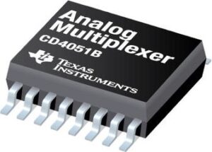
Analog Multiplexer Single 8:1 16-Pin TSSOP T/R, CD4051BQPWRQ1, Texas Instruments

The CD4051B, CD4052B, and CD4053B analog multiplexers are digitally-controlled analog switches that have low ON impedance and very low OFF leakage current. Control of analog signals up to 20 VP-P can be achieved by digital signal amplitudes of 4.5 V to 20 V (If VDD – VSS = 3 V, a VDD – VEE of up to 13 V can be controlled; for VDD – VEE level differences above 13 V, a VDD – VSS of at least 4.5 V is required). For example, if VDD = 4.5 V, VSS = 0 V, and VEE = –13.5 V, analog signals from –13.5 V to 4.5 V can be controlled by digital inputs of 0 V to 5 V. These multiplexer circuits dissipate extremely low quiescent power over the full VDD – VSS and VDD – VEE supply-voltage ranges, independent of the logic state of the control signals. When a logic high (H) is present at the inhibit (INH) input, all channels are off. The CD4051B is a single eight-channel multiplexer that has three binary control inputs (A, B, and C) and an inhibit input. The three binary signals select one of eight channels to be turned on and connect one of the eight inputs to the output. The CD4052B is a differential four-channel multiplexer that has two binary control inputs (A and B) and an inhibit input. The two binary input signals select one of four pairs of channels to be turned on and connect the analog inputs to the outputs. The CD4053B is a triple two-channel multiplexer with three separate digital control inputs (A, B, and C) and an inhibit input. Each control input selects one of a pair of channels, which are connected in a single-pole, double-throw configuration. When these devices are used as demultiplexers, the CHANNEL IN/OUT terminals are the outputs, and the common (COM OUT/IN) terminals are the inputs.

  • Qualified for Automotive Applications
  • Wide Range of Digital and Analog Signal Levels
    • Digital: 3 V to 20 V
    • Analog: = 20 VP-P
  • Low ON Resistance, 125 O (Typ) Over 15 VP-P Signal Input Range for VDD – VEE = 18 V
  • High OFF Resistance, Channel Leakage of ±100 pA (Typ) at VDD – VEE = 18 V
  • Logic-Level Conversion for Digital Addressing Signals of 3 V to 20 V (VDD – VSS = 3 V to 20 V) to Switch Analog Signals to 20 VP-P (VDD – VEE = 20 V)
  • Matched Switching Characteristics, ron = 5 O (Typ) for VDD – VEE = 15 V
  • Very Low Quiescent Power Dissipation Under All Digital-Control Input and Supply Conditions, 0.2 µW (Typ) at VDD – VSS = VDD – VEE = 10 V
  • Binary Address Decoding on Chip
  • 5-V, 10-V, and 15-V Parametric Ratings
  • 100% Tested for Quiescent Current at 20 V
  • Maximum Input Current of 1µA at 18 V Over Full Package Temperature Range, 100 nA at 18 V and 25°C
  • Break-Before-Make Switching Eliminates Channel Overlap
  • Applications
    • Analog and Digital Multiplexing and Demultiplexing
    • Analog-to-Digital (A/D) and Digital-to-Analog (D/A) Conversion
    • Signal Gating
  • Характеристики

    Бренд

    Chip_enable_signals

    Yes

    Max_on_resistance

    1050@5V Ohm

    Number_of_channels_per_chip

    1

    Number_of_outputs_per_chip

    1

    Max_turn_on_time

    720@5V ns

    Output_signal_type

    Single-Ended

    Power_supply_type

    Dual, Single

    Max_propagation_delay_btb

    20@15V ns, 30@10V, 60@5V

    Propagat_delay_test_condit

    50 pF

    Max_on_resist_range

    >=1000 Ohm

    Number_of_inputs_per_chip

    8

    Msl_level

    1

    Конфигурация

    Single 8:1

    Country_of_origin

    United States

    Eccn

    EAR99

    Htsn

    8542390001

    Input_signal_type

    Single

    Kind

    Analog Multiplexer

    Lead_finish

    Gold

    Max_processing_temp

    260

    Mounting

    Surface Mount

    Operat_supply_voltage

    ±10, ±2.5, ±3, ±5, ±9 V, 20, 5

    Operat_temperature

    -40 to 125 °C

    Pin_count

    16

    Product_dimensions

    5.1 x 4.5 x 1.05 mm

    Schedule_b

    8542390000

    Specifications

    http://www.ti.com/general/docs/lit/getliterature.tsp?genericPartNumber=CD4051B-Q1&&fileType=pdf

    Supplier_package

    TSSOP

    Артикул: CD4051BQPWRQ1

    Описание

    The CD4051B, CD4052B, and CD4053B analog multiplexers are digitally-controlled analog switches that have low ON impedance and very low OFF leakage current. Control of analog signals up to 20 VP-P can be achieved by digital signal amplitudes of 4.5 V to 20 V (If VDD – VSS = 3 V, a VDD – VEE of up to 13 V can be controlled; for VDD – VEE level differences above 13 V, a VDD – VSS of at least 4.5 V is required). For example, if VDD = 4.5 V, VSS = 0 V, and VEE = –13.5 V, analog signals from –13.5 V to 4.5 V can be controlled by digital inputs of 0 V to 5 V. These multiplexer circuits dissipate extremely low quiescent power over the full VDD – VSS and VDD – VEE supply-voltage ranges, independent of the logic state of the control signals. When a logic high (H) is present at the inhibit (INH) input, all channels are off. The CD4051B is a single eight-channel multiplexer that has three binary control inputs (A, B, and C) and an inhibit input. The three binary signals select one of eight channels to be turned on and connect one of the eight inputs to the output. The CD4052B is a differential four-channel multiplexer that has two binary control inputs (A and B) and an inhibit input. The two binary input signals select one of four pairs of channels to be turned on and connect the analog inputs to the outputs. The CD4053B is a triple two-channel multiplexer with three separate digital control inputs (A, B, and C) and an inhibit input. Each control input selects one of a pair of channels, which are connected in a single-pole, double-throw configuration. When these devices are used as demultiplexers, the CHANNEL IN/OUT terminals are the outputs, and the common (COM OUT/IN) terminals are the inputs.

  • Qualified for Automotive Applications
  • Wide Range of Digital and Analog Signal Levels
    • Digital: 3 V to 20 V
    • Analog: = 20 VP-P
  • Low ON Resistance, 125 O (Typ) Over 15 VP-P Signal Input Range for VDD – VEE = 18 V
  • High OFF Resistance, Channel Leakage of ±100 pA (Typ) at VDD – VEE = 18 V
  • Logic-Level Conversion for Digital Addressing Signals of 3 V to 20 V (VDD – VSS = 3 V to 20 V) to Switch Analog Signals to 20 VP-P (VDD – VEE = 20 V)
  • Matched Switching Characteristics, ron = 5 O (Typ) for VDD – VEE = 15 V
  • Very Low Quiescent Power Dissipation Under All Digital-Control Input and Supply Conditions, 0.2 µW (Typ) at VDD – VSS = VDD – VEE = 10 V
  • Binary Address Decoding on Chip
  • 5-V, 10-V, and 15-V Parametric Ratings
  • 100% Tested for Quiescent Current at 20 V
  • Maximum Input Current of 1µA at 18 V Over Full Package Temperature Range, 100 nA at 18 V and 25°C
  • Break-Before-Make Switching Eliminates Channel Overlap
  • Applications
    • Analog and Digital Multiplexing and Demultiplexing
    • Analog-to-Digital (A/D) and Digital-to-Analog (D/A) Conversion
    • Signal Gating
  • Детали

    Бренд

    Chip_enable_signals

    Yes

    Max_on_resistance

    1050@5V Ohm

    Number_of_channels_per_chip

    1

    Number_of_outputs_per_chip

    1

    Max_turn_on_time

    720@5V ns

    Output_signal_type

    Single-Ended

    Power_supply_type

    Dual, Single

    Max_propagation_delay_btb

    20@15V ns, 30@10V, 60@5V

    Propagat_delay_test_condit

    50 pF

    Max_on_resist_range

    >=1000 Ohm

    Number_of_inputs_per_chip

    8

    Msl_level

    1

    Конфигурация

    Single 8:1

    Country_of_origin

    United States

    Eccn

    EAR99

    Htsn

    8542390001

    Input_signal_type

    Single

    Kind

    Analog Multiplexer

    Lead_finish

    Gold

    Max_processing_temp

    260

    Mounting

    Surface Mount

    Operat_supply_voltage

    ±10, ±2.5, ±3, ±5, ±9 V, 20, 5

    Operat_temperature

    -40 to 125 °C

    Pin_count

    16

    Product_dimensions

    5.1 x 4.5 x 1.05 mm

    Schedule_b

    8542390000

    Specifications

    http://www.ti.com/general/docs/lit/getliterature.tsp?genericPartNumber=CD4051B-Q1&&fileType=pdf

    Supplier_package

    TSSOP