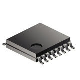
Analog Multiplexer Single 8:1 16-Pin TSSOP T/R, 74HC4051PW-Q100,118, Nexperia

The 74HC4051-Q100; 74HCT4051-Q100 is a high-speed Si-gate CMOS device and is pin compatible with Low-power Schottky TTL (LSTTL). The device is specified in compliance with JEDEC standard no. 7A. The 74HC4051-Q100; 74HCT4051-Q100 is an 8-channel analog multiplexer/demultiplexer with three digital select inputs (S0 to S2), an active-LOW enable input (E), eight independent inputs/outputs (Y0 to Y7) and a common input/output (Z). With E LOW, one of the eight switches is selected (low impedance ON-state) by S0 to S2. With E HIGH, all switches are in the high-impedance OFF-state, independent of S0 to S2. VCC and GND are the supply voltage pins for the digital control inputs (S0 to S2, and E). The VCC to GND ranges are 2.0 V to 10.0 V for 74HC4051-Q100 and 4.5 V to 5.5 V for 74HCT4051-Q100. The analog inputs/outputs (Y0 to Y7, and Z) can swing between VCC as a positive limit and VEE as a negative limit. VCC – VEE may not exceed 10.0 V. For operation as a digital multiplexer/demultiplexer, VEE is connected to GND (typically ground). This product has been qualified to the Automotive Electronics Council (AEC) standard Q100 (Grade 1) and is suitable for use in automotive applications.

  • Automotive product qualification in accordance with AEC-Q100 (Grade 1)
    • Specified from -40 °C to +85 °C and from -40 °C to +125 °C
  • Wide analog input voltage range from -5 V to +5 V
  • Low ON resistance:
    • 80 O (typical) at VCC – VEE = 4.5 V
    • 70 O (typical) at VCC – VEE = 6.0 V
    • 60 O (typical) at VCC – VEE = 9.0 V
  • Logic level translation: to enable 5 V logic to communicate with ±5 V analog signals
  • Typical ‘break before make’ built-in
  • ESD protection:
    • MIL-STD-883, method 3015 exceeds 2000 V
    • HBM JESD22-A114F exceeds 2000 V
    • MM JESD22-A115-A exceeds 200 V (C = 200 pf, R = 0 O)
    • CDM AEC-Q100-011 revision B exceeds 1000 V
  • Multiple package options

Характеристики

Бренд

Number_of_channels_per_chip

1

Number_of_outputs_per_chip

1

Output_signal_type

Single-Ended

Power_supply_type

Dual, Single

Max_propagation_delay_btb

10@6V, 12@4.5V, 60@2V ns, 8@?4.5V

Propagat_delay_test_condit

50 pF

Max_low_lev_output_current

25 mA

Max_on_resist_range

150 to 250 Ohm

Number_of_inputs_per_chip

8

Конфигурация

Single 8:1

Country_of_origin

United States

Eccn

EAR99

Htsn

8541290095

Kind

Analog Multiplexer

Lead_finish

Gold

Max_processing_temp

260

Mounting

Surface Mount

Operat_supply_current

0.016@10V mA

Operat_supply_voltage

±1, ±2.5, ±5, 10, 2, 5 V

Operat_temperature

-40 to 125 °C

Pin_count

16

Product_dimensions

5.1 x 4.5 x 0.95 mm

Schedule_b

8541290080

Specifications

https://4donline.ihs.com/images/VipMasterIC/IC/PHGL/PHGLS25596/PHGLS25596-1.pdf?hkey=52A5661711E402568146F3353EA87419

Артикул: 74HC4051PW-Q100,118

Описание

The 74HC4051-Q100; 74HCT4051-Q100 is a high-speed Si-gate CMOS device and is pin compatible with Low-power Schottky TTL (LSTTL). The device is specified in compliance with JEDEC standard no. 7A. The 74HC4051-Q100; 74HCT4051-Q100 is an 8-channel analog multiplexer/demultiplexer with three digital select inputs (S0 to S2), an active-LOW enable input (E), eight independent inputs/outputs (Y0 to Y7) and a common input/output (Z). With E LOW, one of the eight switches is selected (low impedance ON-state) by S0 to S2. With E HIGH, all switches are in the high-impedance OFF-state, independent of S0 to S2. VCC and GND are the supply voltage pins for the digital control inputs (S0 to S2, and E). The VCC to GND ranges are 2.0 V to 10.0 V for 74HC4051-Q100 and 4.5 V to 5.5 V for 74HCT4051-Q100. The analog inputs/outputs (Y0 to Y7, and Z) can swing between VCC as a positive limit and VEE as a negative limit. VCC – VEE may not exceed 10.0 V. For operation as a digital multiplexer/demultiplexer, VEE is connected to GND (typically ground). This product has been qualified to the Automotive Electronics Council (AEC) standard Q100 (Grade 1) and is suitable for use in automotive applications.

  • Automotive product qualification in accordance with AEC-Q100 (Grade 1)
    • Specified from -40 °C to +85 °C and from -40 °C to +125 °C
  • Wide analog input voltage range from -5 V to +5 V
  • Low ON resistance:
    • 80 O (typical) at VCC – VEE = 4.5 V
    • 70 O (typical) at VCC – VEE = 6.0 V
    • 60 O (typical) at VCC – VEE = 9.0 V
  • Logic level translation: to enable 5 V logic to communicate with ±5 V analog signals
  • Typical ‘break before make’ built-in
  • ESD protection:
    • MIL-STD-883, method 3015 exceeds 2000 V
    • HBM JESD22-A114F exceeds 2000 V
    • MM JESD22-A115-A exceeds 200 V (C = 200 pf, R = 0 O)
    • CDM AEC-Q100-011 revision B exceeds 1000 V
  • Multiple package options

Детали

Бренд

Number_of_channels_per_chip

1

Number_of_outputs_per_chip

1

Output_signal_type

Single-Ended

Power_supply_type

Dual, Single

Max_propagation_delay_btb

10@6V, 12@4.5V, 60@2V ns, 8@?4.5V

Propagat_delay_test_condit

50 pF

Max_low_lev_output_current

25 mA

Max_on_resist_range

150 to 250 Ohm

Number_of_inputs_per_chip

8

Конфигурация

Single 8:1

Country_of_origin

United States

Eccn

EAR99

Htsn

8541290095

Kind

Analog Multiplexer

Lead_finish

Gold

Max_processing_temp

260

Mounting

Surface Mount

Operat_supply_current

0.016@10V mA

Operat_supply_voltage

±1, ±2.5, ±5, 10, 2, 5 V

Operat_temperature

-40 to 125 °C

Pin_count

16

Product_dimensions

5.1 x 4.5 x 0.95 mm

Schedule_b

8541290080

Specifications

https://4donline.ihs.com/images/VipMasterIC/IC/PHGL/PHGLS25596/PHGLS25596-1.pdf?hkey=52A5661711E402568146F3353EA87419