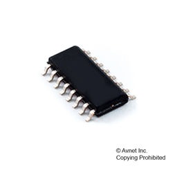
Analog Multiplexer Single 8:1 16-Pin SO T/R, HEF4051BT-Q100,118, Nexperia

The HEF4051B-Q100 is an 8-channel analog multiplexer/demultiplexer with three address inputs (S1 to S3), an active LOW enable input (E), eight independent inputs/outputs (Y0 to Y7) and a common input/output (Z). The device contains eight bidirectional analog switches, each with one side connected to an independent input/output (Y0 to Y7) and the other side connected to a common input/output (Z). With E LOW, one of the eight switches is selected (low-impedance ON-state) by S1 to S3. With E HIGH, all switches are in the high-impedance OFF-state, independent of S1 to S3. If break before make is needed, then it is necessary to use the enable input. VDD and VSS are the supply voltage connections for the digital control inputs (S1 to S3, and E). The VDD to VSS range is 3 V to 15 V. The analog inputs/outputs (Y0 to Y7, and Z) can swing between VDD as a positive limit and VEE as a negative limit. VDD – VEE may not exceed 15 V. Unused inputs must be connected to VDD, VSS, or another input. For operation as a digital multiplexer/demultiplexer, VEE is connected to VSS (typically ground). VEE and VSS are the supply voltage connections for the switches. This product has been qualified to the Automotive Electronics Council (AEC) standard Q100 (Grade 1) and is suitable for use in automotive applications.

  • Automotive product qualification in accordance with AEC-Q100 (Grade 1)
    • Specified from -40 °C to +85 °C and from -40 °C to +125 °C
  • Fully static operation
  • 5 V, 10 V, and 15 V parametric ratings
  • Standardized symmetrical output characteristics
  • ESD protection:
    • MIL-STD-833, method 3015 exceeds 2000 V
    • HBM JESD22-A114F exceeds 2000 V
    • MM JESD22-A115-A exceeds 200 V (C = 200 pF, R = 0 O)
  • Complies with JEDEC standard JESD 13-B
Характеристики

Бренд

Chip_enable_signals

Yes

Max_on_resistance

2500@5V Ohm

Number_of_channels_per_chip

1

Number_of_outputs_per_chip

1

Max_turn_on_time

280@5V ns

Output_signal_type

Single-Ended

Power_supply_type

Single

Max_propagation_delay_btb

130@10V, 300@5V ns, 90@15V

Max_low_lev_output_current

10 mA

Max_on_resist_range

>=1000 Ohm

Number_of_inputs_per_chip

8

Max_high_lev_output_current

10 mA

Msl_level

1

Конфигурация

Single 8:1

Country_of_origin

Thailand

Eccn

EAR99

Htsn

8542390001

Input_signal_type

Single

Kind

Analog Multiplexer

Lead_finish

Gold

Max_power_dissipation

500 mW

Max_processing_temp

260

Mounting

Surface Mount

Operat_supply_current

0.005@5V mA

Operat_supply_voltage

15, 3 V

Operat_temperature

-40 to 125 °C

Pin_count

16

Product_dimensions

10 x 4 x 1.45 mm

Schedule_b

8542390000

Specifications

https://4donline.ihs.com/images/VipMasterIC/IC/NEXP/NEXP-S-A0003059912/NEXP-S-A0003059912-1.pdf?hkey=52A5661711E402568146F3353EA87419

Supplier_package

SO

Артикул: HEF4051BT-Q100,118

Описание

The HEF4051B-Q100 is an 8-channel analog multiplexer/demultiplexer with three address inputs (S1 to S3), an active LOW enable input (E), eight independent inputs/outputs (Y0 to Y7) and a common input/output (Z). The device contains eight bidirectional analog switches, each with one side connected to an independent input/output (Y0 to Y7) and the other side connected to a common input/output (Z). With E LOW, one of the eight switches is selected (low-impedance ON-state) by S1 to S3. With E HIGH, all switches are in the high-impedance OFF-state, independent of S1 to S3. If break before make is needed, then it is necessary to use the enable input. VDD and VSS are the supply voltage connections for the digital control inputs (S1 to S3, and E). The VDD to VSS range is 3 V to 15 V. The analog inputs/outputs (Y0 to Y7, and Z) can swing between VDD as a positive limit and VEE as a negative limit. VDD – VEE may not exceed 15 V. Unused inputs must be connected to VDD, VSS, or another input. For operation as a digital multiplexer/demultiplexer, VEE is connected to VSS (typically ground). VEE and VSS are the supply voltage connections for the switches. This product has been qualified to the Automotive Electronics Council (AEC) standard Q100 (Grade 1) and is suitable for use in automotive applications.

  • Automotive product qualification in accordance with AEC-Q100 (Grade 1)
    • Specified from -40 °C to +85 °C and from -40 °C to +125 °C
  • Fully static operation
  • 5 V, 10 V, and 15 V parametric ratings
  • Standardized symmetrical output characteristics
  • ESD protection:
    • MIL-STD-833, method 3015 exceeds 2000 V
    • HBM JESD22-A114F exceeds 2000 V
    • MM JESD22-A115-A exceeds 200 V (C = 200 pF, R = 0 O)
  • Complies with JEDEC standard JESD 13-B
Детали

Бренд

Chip_enable_signals

Yes

Max_on_resistance

2500@5V Ohm

Number_of_channels_per_chip

1

Number_of_outputs_per_chip

1

Max_turn_on_time

280@5V ns

Output_signal_type

Single-Ended

Power_supply_type

Single

Max_propagation_delay_btb

130@10V, 300@5V ns, 90@15V

Max_low_lev_output_current

10 mA

Max_on_resist_range

>=1000 Ohm

Number_of_inputs_per_chip

8

Max_high_lev_output_current

10 mA

Msl_level

1

Конфигурация

Single 8:1

Country_of_origin

Thailand

Eccn

EAR99

Htsn

8542390001

Input_signal_type

Single

Kind

Analog Multiplexer

Lead_finish

Gold

Max_power_dissipation

500 mW

Max_processing_temp

260

Mounting

Surface Mount

Operat_supply_current

0.005@5V mA

Operat_supply_voltage

15, 3 V

Operat_temperature

-40 to 125 °C

Pin_count

16

Product_dimensions

10 x 4 x 1.45 mm

Schedule_b

8542390000

Specifications

https://4donline.ihs.com/images/VipMasterIC/IC/NEXP/NEXP-S-A0003059912/NEXP-S-A0003059912-1.pdf?hkey=52A5661711E402568146F3353EA87419

Supplier_package

SO