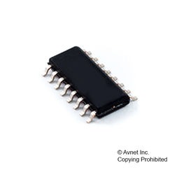
Analog Multiplexer Single 8:1 16-Pin SO T/R, HCF4051YM013TR, STMicroelectronics

The HCF4051 device is a monolithic integrated circuit fabricated in MOS (metal oxide semiconductor) technology available in SO-16 and PDIP-16 packages.The HCF4051 analog multiplexer/demultiplexer is a digitally controlled analog switch having low ON impedance and very low OFF leakage current. This multiplexer circuit dissipates extremely low quiescent power over the full VDD- VSSand VDD- VEEsupply voltage range, independent of the logic state of the control signals.This device is a single 8-channel multiplexer having three binary control inputs, A, B, and C, and an inhibit input. The three binary signals select 1 of 8 channels to be turned on, and connect one of the 8 inputs to the output. When a logic “1” is present at the inhibit input terminal all channels are off.

  • Low “ON” resistance: 125 O (typ.)
  • Over 15 V p.p signal-input range for VDD– VEE= 15 V
  • High “OFF” resistance, channel leakage: ± 100 pA (typ.) at VDD– VEE= 18 V
  • Binary address decoding on chip
  • High degree of linearity: < 0.5="" %="" distortion="" typ.="" at="">IS= 1 KHz, VIS= 5 Vpp, VDD– VSS= 10 V, RL= 10 kO
  • Very low quiescent power dissipation under all digital control input and supply conditions: 0.2 µW (typ.) VDD– VSS= VDD– VEE= 10 V
  • Matched switch characteristics: RON= 5 O (typ.) for VDD– VEE= 15 V
  • Wide range of digital and analog signal levels: digital 3 to 20, analog to 20 V p.p.
  • Quiescent current specified up to 20 V
  • 5 V, 10 V and 15 V parametric ratings
  • ESD performance
  • HBM: 2 kV
  • MM: 200 V
  • CDM: 750 V
  • Input leakage current II= 100 nA (max.) at VDD= 18 V, TA= 25 °C
  • 100 % tested for quiescent current
  • Характеристики

    Бренд

    Chip_enable_signals

    Yes

    Max_on_resistance

    1050@5V Ohm

    Number_of_channels_per_chip

    1

    Number_of_outputs_per_chip

    1

    Max_turn_on_time

    720@5V ns

    Output_signal_type

    Single-Ended

    Power_supply_type

    Single

    Max_propagation_delay_btb

    20@15V, 30@10V, 60@5V ns

    Propagat_delay_test_condit

    50 pF

    Max_frequency_25_deg_c_vcc

    60@5 MHz

    Number_of_inputs_per_chip

    8

    Msl_level

    3

    Конфигурация

    Single 8:1

    Country_of_origin

    China

    Eccn

    EAR99

    Htsn

    8542330001

    Input_signal_type

    Single

    Kind

    Analog Multiplexer

    Lead_finish

    Gold Over Nickel Palladium

    Max_power_dissipation

    500 mW

    Max_processing_temp

    260

    Mounting

    Surface Mount

    Operat_supply_voltage

    20, 3 V

    Operat_temperature

    -40 to 125 °C

    Pin_count

    16

    Product_dimensions

    10(Max) x 4(Max) x 1.65(Max)

    Schedule_b

    8542330000

    Screening_level

    Automotive

    Specifications

    https://4donline.ihs.com/images/VipMasterIC/IC/SGST/SGSTS48885/SGSTS48885-1.pdf?hkey=52A5661711E402568146F3353EA87419

    Supplier_package

    SO

    Артикул: HCF4051YM013TR

    Описание

    The HCF4051 device is a monolithic integrated circuit fabricated in MOS (metal oxide semiconductor) technology available in SO-16 and PDIP-16 packages.The HCF4051 analog multiplexer/demultiplexer is a digitally controlled analog switch having low ON impedance and very low OFF leakage current. This multiplexer circuit dissipates extremely low quiescent power over the full VDD- VSSand VDD- VEEsupply voltage range, independent of the logic state of the control signals.This device is a single 8-channel multiplexer having three binary control inputs, A, B, and C, and an inhibit input. The three binary signals select 1 of 8 channels to be turned on, and connect one of the 8 inputs to the output. When a logic “1” is present at the inhibit input terminal all channels are off.

  • Low “ON” resistance: 125 O (typ.)
  • Over 15 V p.p signal-input range for VDD– VEE= 15 V
  • High “OFF” resistance, channel leakage: ± 100 pA (typ.) at VDD– VEE= 18 V
  • Binary address decoding on chip
  • High degree of linearity: < 0.5="" %="" distortion="" typ.="" at="">IS= 1 KHz, VIS= 5 Vpp, VDD– VSS= 10 V, RL= 10 kO
  • Very low quiescent power dissipation under all digital control input and supply conditions: 0.2 µW (typ.) VDD– VSS= VDD– VEE= 10 V
  • Matched switch characteristics: RON= 5 O (typ.) for VDD– VEE= 15 V
  • Wide range of digital and analog signal levels: digital 3 to 20, analog to 20 V p.p.
  • Quiescent current specified up to 20 V
  • 5 V, 10 V and 15 V parametric ratings
  • ESD performance
  • HBM: 2 kV
  • MM: 200 V
  • CDM: 750 V
  • Input leakage current II= 100 nA (max.) at VDD= 18 V, TA= 25 °C
  • 100 % tested for quiescent current
  • Детали

    Бренд

    Chip_enable_signals

    Yes

    Max_on_resistance

    1050@5V Ohm

    Number_of_channels_per_chip

    1

    Number_of_outputs_per_chip

    1

    Max_turn_on_time

    720@5V ns

    Output_signal_type

    Single-Ended

    Power_supply_type

    Single

    Max_propagation_delay_btb

    20@15V, 30@10V, 60@5V ns

    Propagat_delay_test_condit

    50 pF

    Max_frequency_25_deg_c_vcc

    60@5 MHz

    Number_of_inputs_per_chip

    8

    Msl_level

    3

    Конфигурация

    Single 8:1

    Country_of_origin

    China

    Eccn

    EAR99

    Htsn

    8542330001

    Input_signal_type

    Single

    Kind

    Analog Multiplexer

    Lead_finish

    Gold Over Nickel Palladium

    Max_power_dissipation

    500 mW

    Max_processing_temp

    260

    Mounting

    Surface Mount

    Operat_supply_voltage

    20, 3 V

    Operat_temperature

    -40 to 125 °C

    Pin_count

    16

    Product_dimensions

    10(Max) x 4(Max) x 1.65(Max)

    Schedule_b

    8542330000

    Screening_level

    Automotive

    Specifications

    https://4donline.ihs.com/images/VipMasterIC/IC/SGST/SGSTS48885/SGSTS48885-1.pdf?hkey=52A5661711E402568146F3353EA87419

    Supplier_package

    SO