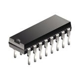
Analog Multiplexer Single 4:1 16-Pin PDIP, DG509BEJ-E3, Vishay

The DG509B is a dual 4-channel differential analog multiplexer designed to connect one of four differential inputs to a common dual output as determined by its 2-bit binary address (A0, A1). Break-before-make switching action protects against momentary crosstalk between adjacent channels. An on channel conducts current equally well in both directions. In the off state each channel blocks voltages up to the power supply rails. An enable (EN) function allows the user to reset the multiplexer / demultiplexer to all switches off for stacking several devices. All control inputs, addresses (AX) and enable (EN) are TTL compatible over the full specified operating temperature range. The DG509B is fabricated on an enhanced SG-II CMOS process that achieves improved performance on: reduced charge injection, lower device leakage, and minimized parasitic capacitance. As the DG509B has a long history in the industry with many suppliers offering copies – and in some cases improved variations – with the best in class improvements. Applications for the DG509B include high speed and high precision data acquisition, audio signal switching and routing, ATE systems, and avionics. High performance and low power dissipation make them ideal for battery operated and remote instrumentation applications. The DG509B have the absolute maximum voltage rating extended to 44 V. Additionally, single supply operation is also allowed. An epitaxial layer prevents latch-up. The DG509B are both available in 16-lead SOIC, TSSOP, PDIP, and miniQFN (1.8 mm x 2.6 mm) package options with extended temperature range of -40°C to +125°C.

  • Operate with single or dual power supply
  • V+ to V- analog signal swing range
  • 44 V power supply maximum rating
  • Extended operate temperature range: -40 °C to +125 °C
  • Low leakage typically < 3 pA
  • Low charge injection – QINJ = 2 pC
  • Low power – ISUPPLY: 10 µA
  • TTL compatible logic
  • > 250 mA latch-up current per JESD78
  • Available in SOIC16, TSSOP16, PDIP, and miniQFN16 packages
  • Superior alternative to:
    • ADG509A, DG509A, HI-509

Характеристики

Бренд

Chip_enable_signals

Yes

Max_on_resistance

500@12V Ohm

Number_of_channels_per_chip

1

Number_of_outputs_per_chip

2

Max_turn_on_time

300@12V ns

Output_signal_type

Differential

Power_supply_type

Dual, Single

Max_propagation_delay_btb

300@±15V, 400@12V ns

Propagat_delay_test_condit

35 pF

Max_on_resist_range

400 to 1000 Ohm

Number_of_inputs_per_chip

8

Max_high_lev_output_current

30 mA

Конфигурация

Single 4:1

Eccn

EAR99

Htsn

8542390001

Input_signal_type

Differential

Kind

Analog Multiplexer

Max_power_dissipation

510 mW

Mounting

Through Hole

Operat_supply_current

0.5@15V

Operat_supply_voltage

±12, ±15, ±18 V, ±20, ±5, ±9, 12, 44

Operat_temperature

-40 to 125 °C

Pin_count

16

Product_dimensions

20.07 x 6.81 x 3.81 mm

Schedule_b

8542390000

Screening_level

Extended

Specifications

http://www.vishay.com/docs/64821/dg508b.pdf

Supplier_package

PDIP

Артикул: DG509BEJ-E3

Описание

The DG509B is a dual 4-channel differential analog multiplexer designed to connect one of four differential inputs to a common dual output as determined by its 2-bit binary address (A0, A1). Break-before-make switching action protects against momentary crosstalk between adjacent channels. An on channel conducts current equally well in both directions. In the off state each channel blocks voltages up to the power supply rails. An enable (EN) function allows the user to reset the multiplexer / demultiplexer to all switches off for stacking several devices. All control inputs, addresses (AX) and enable (EN) are TTL compatible over the full specified operating temperature range. The DG509B is fabricated on an enhanced SG-II CMOS process that achieves improved performance on: reduced charge injection, lower device leakage, and minimized parasitic capacitance. As the DG509B has a long history in the industry with many suppliers offering copies – and in some cases improved variations – with the best in class improvements. Applications for the DG509B include high speed and high precision data acquisition, audio signal switching and routing, ATE systems, and avionics. High performance and low power dissipation make them ideal for battery operated and remote instrumentation applications. The DG509B have the absolute maximum voltage rating extended to 44 V. Additionally, single supply operation is also allowed. An epitaxial layer prevents latch-up. The DG509B are both available in 16-lead SOIC, TSSOP, PDIP, and miniQFN (1.8 mm x 2.6 mm) package options with extended temperature range of -40°C to +125°C.

  • Operate with single or dual power supply
  • V+ to V- analog signal swing range
  • 44 V power supply maximum rating
  • Extended operate temperature range: -40 °C to +125 °C
  • Low leakage typically < 3 pA
  • Low charge injection – QINJ = 2 pC
  • Low power – ISUPPLY: 10 µA
  • TTL compatible logic
  • > 250 mA latch-up current per JESD78
  • Available in SOIC16, TSSOP16, PDIP, and miniQFN16 packages
  • Superior alternative to:
    • ADG509A, DG509A, HI-509

Детали

Бренд

Chip_enable_signals

Yes

Max_on_resistance

500@12V Ohm

Number_of_channels_per_chip

1

Number_of_outputs_per_chip

2

Max_turn_on_time

300@12V ns

Output_signal_type

Differential

Power_supply_type

Dual, Single

Max_propagation_delay_btb

300@±15V, 400@12V ns

Propagat_delay_test_condit

35 pF

Max_on_resist_range

400 to 1000 Ohm

Number_of_inputs_per_chip

8

Max_high_lev_output_current

30 mA

Конфигурация

Single 4:1

Eccn

EAR99

Htsn

8542390001

Input_signal_type

Differential

Kind

Analog Multiplexer

Max_power_dissipation

510 mW

Mounting

Through Hole

Operat_supply_current

0.5@15V

Operat_supply_voltage

±12, ±15, ±18 V, ±20, ±5, ±9, 12, 44

Operat_temperature

-40 to 125 °C

Pin_count

16

Product_dimensions

20.07 x 6.81 x 3.81 mm

Schedule_b

8542390000

Screening_level

Extended

Specifications

http://www.vishay.com/docs/64821/dg508b.pdf

Supplier_package

PDIP