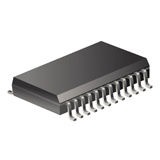
Analog Multiplexer Single 16:1 24-Pin SOIC Tube, CD4067BM, Texas Instruments

CD4067B and CD4097B CMOS analog multiplexers/demultiplexers* are digitally controlled analog switches having low ON impedance, low OFF leakage current, and internal address decoding.In addition, the ON resistance is relatively constant over the full input-signal range.The CD4067B is a 16-channel multiplexer with four binary control inputs, A, B, C, D, and an inhibit input, arranged so that any combination of the inputs selects one switch. The CD4097B is a differential 8-channel multiplexer having three binary control inputs, A, B, C, and an inhibit input.The inputs permit selection of one of eight pairs of switches. A logic “1” present at the inhibit input turns all channels off. The CD4067B and CD4097B types are supplied in 24-lead hermetic dual-in-line ceramic packages (F3A suffix), 24-lead dual-in-line plastic packages (E suffix), 24-lead small-outline packages (M, M96, and NSR suffixes), and 24-lead thin shrink small-outline packages (P and PWR suffixes).

  • Low ON resistance: 125 O (typ.) over 15 Vp-p signal-input range for VDD – VSS = 15 V
  • High OFF resistance: channel leakage of ±10 pA (typ.) @ VDD – VSS = 10 V
  • Matched switch characteristics: RON = 5O (typ.) for VDD – VSS = 15 V
  • Very low quiescent power dissipation under all digital-control input and supply conditions: 0.2 uW (typ.) @ VDD – VSS = 10 V
  • Binary address decoding on chip
  • 5-V, 10-V, and 15-V parametric ratings
  • 100% tested for quiescent current at 20 V
  • Maximum input current of 1 µA at 18 V over full package-temperature range; 100nA at 18 V and 25°C
  • Meets all requirements of JEDEC Tentative Standard No. 13A, “Standard Specifications for Description of "B" Series CMOS Devices”
  • Applications:
    • Analog and digital multiplexing and demultiplexing
    • A/D and D/A conversion
    • Siganl gating
  • Характеристики

    Бренд

    Country_of_origin

    Taiwan

    Max_on_resistance

    1050@5V Ohm

    Number_of_channels_per_chip

    1

    Number_of_outputs_per_chip

    1

    Max_turn_on_time

    650@5V ns

    Output_signal_type

    Single-Ended

    Power_supply_type

    Single

    Max_propagation_delay_btb

    20@15V, 30@10V, 60@5V ns

    Propagat_delay_test_condit

    50 pF

    Max_on_resist_range

    >=1000 Ohm

    Number_of_inputs_per_chip

    16

    Msl_level

    1

    Конфигурация

    Single 16:1

    Chip_enable_signals

    Yes

    Htsn

    8542390001

    Eccn

    EAR99

    Input_signal_type

    Single

    Kind

    Analog Multiplexer

    Lead_finish

    Gold

    Max_power_dissipation

    500 mW

    Max_processing_temp

    260, 265

    Mounting

    Surface Mount

    Operat_supply_voltage

    18, 3 V

    Operat_temperature

    -55 to 125 °C

    Pin_count

    24

    Product_dimensions

    15.4 x 7.52 x 2.35 mm

    Schedule_b

    8542390000

    Specifications

    http://www.ti.com/general/docs/lit/getliterature.tsp?genericPartNumber=CD4067B-MIL&&fileType=pdf

    Supplier_package

    SOIC

    Артикул: CD4067BM

    Описание

    CD4067B and CD4097B CMOS analog multiplexers/demultiplexers* are digitally controlled analog switches having low ON impedance, low OFF leakage current, and internal address decoding.In addition, the ON resistance is relatively constant over the full input-signal range.The CD4067B is a 16-channel multiplexer with four binary control inputs, A, B, C, D, and an inhibit input, arranged so that any combination of the inputs selects one switch. The CD4097B is a differential 8-channel multiplexer having three binary control inputs, A, B, C, and an inhibit input.The inputs permit selection of one of eight pairs of switches. A logic “1” present at the inhibit input turns all channels off. The CD4067B and CD4097B types are supplied in 24-lead hermetic dual-in-line ceramic packages (F3A suffix), 24-lead dual-in-line plastic packages (E suffix), 24-lead small-outline packages (M, M96, and NSR suffixes), and 24-lead thin shrink small-outline packages (P and PWR suffixes).

  • Low ON resistance: 125 O (typ.) over 15 Vp-p signal-input range for VDD – VSS = 15 V
  • High OFF resistance: channel leakage of ±10 pA (typ.) @ VDD – VSS = 10 V
  • Matched switch characteristics: RON = 5O (typ.) for VDD – VSS = 15 V
  • Very low quiescent power dissipation under all digital-control input and supply conditions: 0.2 uW (typ.) @ VDD – VSS = 10 V
  • Binary address decoding on chip
  • 5-V, 10-V, and 15-V parametric ratings
  • 100% tested for quiescent current at 20 V
  • Maximum input current of 1 µA at 18 V over full package-temperature range; 100nA at 18 V and 25°C
  • Meets all requirements of JEDEC Tentative Standard No. 13A, “Standard Specifications for Description of "B" Series CMOS Devices”
  • Applications:
    • Analog and digital multiplexing and demultiplexing
    • A/D and D/A conversion
    • Siganl gating
  • Детали

    Бренд

    Country_of_origin

    Taiwan

    Max_on_resistance

    1050@5V Ohm

    Number_of_channels_per_chip

    1

    Number_of_outputs_per_chip

    1

    Max_turn_on_time

    650@5V ns

    Output_signal_type

    Single-Ended

    Power_supply_type

    Single

    Max_propagation_delay_btb

    20@15V, 30@10V, 60@5V ns

    Propagat_delay_test_condit

    50 pF

    Max_on_resist_range

    >=1000 Ohm

    Number_of_inputs_per_chip

    16

    Msl_level

    1

    Конфигурация

    Single 16:1

    Chip_enable_signals

    Yes

    Htsn

    8542390001

    Eccn

    EAR99

    Input_signal_type

    Single

    Kind

    Analog Multiplexer

    Lead_finish

    Gold

    Max_power_dissipation

    500 mW

    Max_processing_temp

    260, 265

    Mounting

    Surface Mount

    Operat_supply_voltage

    18, 3 V

    Operat_temperature

    -55 to 125 °C

    Pin_count

    24

    Product_dimensions

    15.4 x 7.52 x 2.35 mm

    Schedule_b

    8542390000

    Specifications

    http://www.ti.com/general/docs/lit/getliterature.tsp?genericPartNumber=CD4067B-MIL&&fileType=pdf

    Supplier_package

    SOIC