Описание
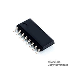
The HCF4052B is a monolithic integrated circuit fabricated in Metal Oxide Semiconductor technology available in DIP and SOP packages.The HCF4052B analog Multiplexer/demultiplexer is a digitally controlled analog switch having low ON impedance and very low OFF leakage current. This multiplexer circuit dissipate extremely low quiescent power over the full VDD – VSS and VDD – VEE supply voltage range, independent of the logic state of the control signals.When a logic “1” is present at the inhibit input terminal all channel are off. This device is a differential 4-channel multiplexer having two binary control inputs, A and B and an inhibit input.The two binary input signals selects 1 of 4 pairs of channels to be turned on and connect the analog inputs to the outputs.
- LOW “ON” RESISTANCE : 125? (Typ.) OVER 15V p.p SIGNAL-INPUT RANGE FOR VDD – VEE = 15V
- HIGH “OFF” RESISTANCE : CHANNEL LEAKAGE ± 100pA (Typ.) at VDD – VEE = 18V
- BINARY ADDRESS DECODING ON CHIP
- HIGH DEGREE OF LINEARITY : < 0.5% DISTORTION TYP. at fIS = 1KHz, VIS =5Vpp, VDD - VSS > 10V, RL = 10K?
- VERY LOW QUIESCENT POWER DISSIPATION UNDER ALL DIGITAL CONTROL INPUT AND SUPPLY CONDITIONS : 0.2 µW (Typ.) at VDD – VSS = VDD – VEE =10V
- MATCHED SWITCH CHARACTERISTICS : RON = 5? (Typ.) FOR VDD – VEE = 15V
- WIDE RANGE OF DIGITAL AND ANALOG SIGNAL LEVELS : DIGITAL 3 to 20, ANALOG TO 20V p.p.
- QUIESCENT CURRENT SPECIF. UP TO 20V
- 5V, 10V AND 15V PARAMETRIC RATINGS
- INPUT LEAKAGE CURRENT II = 100nA (MAX) AT VDD = 18V TA = 25°C
- 100% TESTED FOR QUIESCENT CURRENT
- MEETS ALL REQUIREMENTS OF JEDEC JESD13B ” STANDARD SPECIFICATIONS FOR DESCRIPTION OF B SERIES CMOS DEVICES