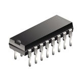
Analog Multiplexer Dual 4:1 16-Pin PDIP Tube, HCF4052BEY, STMicroelectronics

The HCF4052B is a monolithic integrated circuit fabricated in Metal Oxide Semiconductor technology available in DIP and SOP packages. The HCF4052B analog multiplexer/demultiplexer is a digitally controlled analog switch having low ON impedance and very low OFF leakage current. This multiplexer circuit dissipate extremely low quiescent power over the full VDD – VSS and VDD – VEE supply voltage range, independent of the logic state of the control signals.When a logic “1” is present at the inhibit input terminal all channel are off. This device is a differential 4-channel multiplexer having two binary control inputs, A and B and an inhibit input. The two binary input signals selects 1 of 4 pairs of channels to be turned on and connect the analog inputs to the outputs.

  • LOW “ON” RESISTANCE : 125? (Typ.) OVER 15V p.p SIGNAL-INPUT RANGE FOR VDD – VEE = 15V
  • HIGH “OFF” RESISTANCE : CHANNEL LEAKAGE ± 100pA (Typ.) at VDD – VEE = 18V
  • BINARY ADDRESS DECODING ON CHIP
  • HIGH DEGREE OF LINEARITY : < 0.5% DISTORTION TYP. at fIS = 1KHz, VIS =5Vpp, VDD - VSS > 10V, RL = 10K?
  • VERY LOW QUIESCENT POWER DISSIPATION UNDER ALL DIGITAL CONTROL INPUT AND SUPPLY CONDITIONS : 0.2 µW (Typ.) at VDD – VSS = VDD – VEE =10V
  • MATCHED SWITCH CHARACTERISTICS : RON = 5? (Typ.) FOR VDD – VEE = 15V
  • WIDE RANGE OF DIGITAL AND ANALOG SIGNAL LEVELS : DIGITAL 3 to 20, ANALOG TO 20V p.p.
  • QUIESCENT CURRENT SPECIF. UP TO 20V
  • 5V, 10V AND 15V PARAMETRIC RATINGS
  • INPUT LEAKAGE CURRENT II = 100nA (MAX) AT VDD = 18V TA = 25°C
  • 100% TESTED FOR QUIESCENT CURRENT
  • MEETS ALL REQUIREMENTS OF JEDEC JESD13B ” STANDARD SPECIFICATIONS FOR DESCRIPTION OF B SERIES CMOS DEVICES
Характеристики

Бренд

Chip_enable_signals

Yes

Max_on_resistance

1050@5V Ohm

Number_of_channels_per_chip

2

Number_of_outputs_per_chip

2

Max_turn_on_time

720@5V ns

Output_signal_type

Single-Ended

Power_supply_type

Single

Max_propagation_delay_btb

20@15V, 30@10V, 60@5V ns

Propagat_delay_test_condit

50 pF

Max_on_resist_range

>=1000 Ohm

Number_of_inputs_per_chip

8

Конфигурация

Dual 4:1

Eccn

EAR99

Htsn

8542310001

Input_signal_type

Single

Kind

Analog Multiplexer

Lead_finish

Gold

Max_power_dissipation

500 mW

Mounting

Through Hole

Operat_supply_voltage

20, 3 V

Operat_temperature

-55 to 125 °C

Pin_count

16

Product_dimensions

20 x 7.1 x 5.1 mm

Schedule_b

8542310000

Specifications

https://4donline.ihs.com/images/VipMasterIC/IC/SGST/SGSTS31717/SGSTS31717-1.pdf?hkey=52A5661711E402568146F3353EA87419

Supplier_package

PDIP

Артикул: HCF4052BEY

Описание

The HCF4052B is a monolithic integrated circuit fabricated in Metal Oxide Semiconductor technology available in DIP and SOP packages. The HCF4052B analog multiplexer/demultiplexer is a digitally controlled analog switch having low ON impedance and very low OFF leakage current. This multiplexer circuit dissipate extremely low quiescent power over the full VDD – VSS and VDD – VEE supply voltage range, independent of the logic state of the control signals.When a logic “1” is present at the inhibit input terminal all channel are off. This device is a differential 4-channel multiplexer having two binary control inputs, A and B and an inhibit input. The two binary input signals selects 1 of 4 pairs of channels to be turned on and connect the analog inputs to the outputs.

  • LOW “ON” RESISTANCE : 125? (Typ.) OVER 15V p.p SIGNAL-INPUT RANGE FOR VDD – VEE = 15V
  • HIGH “OFF” RESISTANCE : CHANNEL LEAKAGE ± 100pA (Typ.) at VDD – VEE = 18V
  • BINARY ADDRESS DECODING ON CHIP
  • HIGH DEGREE OF LINEARITY : < 0.5% DISTORTION TYP. at fIS = 1KHz, VIS =5Vpp, VDD - VSS > 10V, RL = 10K?
  • VERY LOW QUIESCENT POWER DISSIPATION UNDER ALL DIGITAL CONTROL INPUT AND SUPPLY CONDITIONS : 0.2 µW (Typ.) at VDD – VSS = VDD – VEE =10V
  • MATCHED SWITCH CHARACTERISTICS : RON = 5? (Typ.) FOR VDD – VEE = 15V
  • WIDE RANGE OF DIGITAL AND ANALOG SIGNAL LEVELS : DIGITAL 3 to 20, ANALOG TO 20V p.p.
  • QUIESCENT CURRENT SPECIF. UP TO 20V
  • 5V, 10V AND 15V PARAMETRIC RATINGS
  • INPUT LEAKAGE CURRENT II = 100nA (MAX) AT VDD = 18V TA = 25°C
  • 100% TESTED FOR QUIESCENT CURRENT
  • MEETS ALL REQUIREMENTS OF JEDEC JESD13B ” STANDARD SPECIFICATIONS FOR DESCRIPTION OF B SERIES CMOS DEVICES
Детали

Бренд

Chip_enable_signals

Yes

Max_on_resistance

1050@5V Ohm

Number_of_channels_per_chip

2

Number_of_outputs_per_chip

2

Max_turn_on_time

720@5V ns

Output_signal_type

Single-Ended

Power_supply_type

Single

Max_propagation_delay_btb

20@15V, 30@10V, 60@5V ns

Propagat_delay_test_condit

50 pF

Max_on_resist_range

>=1000 Ohm

Number_of_inputs_per_chip

8

Конфигурация

Dual 4:1

Eccn

EAR99

Htsn

8542310001

Input_signal_type

Single

Kind

Analog Multiplexer

Lead_finish

Gold

Max_power_dissipation

500 mW

Mounting

Through Hole

Operat_supply_voltage

20, 3 V

Operat_temperature

-55 to 125 °C

Pin_count

16

Product_dimensions

20 x 7.1 x 5.1 mm

Schedule_b

8542310000

Specifications

https://4donline.ihs.com/images/VipMasterIC/IC/SGST/SGSTS31717/SGSTS31717-1.pdf?hkey=52A5661711E402568146F3353EA87419

Supplier_package

PDIP