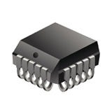
ADC Single SAR 75ksps 8-bit Serial 20-Pin PLCC Tube, TLC540IFN, Texas Instruments

The TLC540 and TLC541 are CMOS A/ D converters built around an 8-bit switched-capacitor successive-approximation A/D converters. They are designed for serial interface to a microprocessor or peripheral via a 3-state output with up to four control inputs, including independent SYSTEM CLOCK, I/O CLOCK, chip select (CS), and ADDRESS INPUT. A 4-MHz system clock for the TLC540 and a 2.1-MHz system clock for the TLC541 with a design that includes simultaneous read/write operation allow high-speed data transfers and sample rates of up to 75,180 samples per second for the TLC540 and 40,000 samples per second for the TLC541. In addition to the high-speed converter and versatile control logic, there is an on-chip 12-channel analog multiplexer that can be used to sample any one of 11 inputs or an internal self-test voltage, and a sample-and-hold that can operate automatically or under microprocessor control. The converters incorporated in the TLC540 and TLC541 feature differential high-impedance reference inputs that facilitate ratiometric conversion, scaling, and analog circuitry isolation from logic and supply noises. A switched-capacitor design allows low-error (±0.5 LSB) conversion in 9 us for the TLC540 and 17 us for the TLC541 over the full operating temperature range. The TLC540I and TLC541I are characterized for operation from -40°C to 85°C.The TLC541M is characterized for operation from -55°C to 125°C.
  • 8-Bit Resolution A/D Converter
  • Microprocessor Peripheral or Stand-Alone Operation
  • On-Chip 12-Channel Analog Multiplexer
  • Built-In Self-Test Mode
  • Software-Controllable Sample and Hold
  • Total Unadjusted Error … ±0.5 LSB Max
  • TLC541 Is Direct Replacement for Motorola MC145040 and National Semiconductor ADC0811. TLC540 Is Capable of Higher Speed
  • Pinout and Control Signals Compatible With TLC1540 Family of 10-Bit A/D Converters
  • CMOS Technology
  • Характеристики

    Volt_supply_source

    Single

    Eccn

    EAR99

    Sampling_rate

    75 ksps

    Volt_reference

    External

    Digital_supply_support

    No

    Architecture

    SAR

    Resolution

    8 Bit

    Differential_nonlinearity

    0.5 LSB

    Input_type

    Voltage

    Input_signal_type

    Single-Ended

    Input_volt

    5 V

    Бренд

    Msl_level

    1

    Country_of_origin

    United States

    Number_of_analog_inputs

    11

    Lead_finish

    Matte Tin

    Htsn

    8542390001

    Max_power_dissipation

    12.5 mW

    Max_processing_temp

    260

    Mounting

    Surface Mount

    Operating_temp

    -40 to 85 °C

    Pin_count

    20

    Product_dimensions

    8.96 x 8.96 x 4.06 mm

    Schedule_b

    8542390000

    Specifications

    http://www.ti.com/general/docs/lit/getliterature.tsp?genericPartNumber=TLC540&&fileType=pdf

    Supplier_package

    PLCC

    Polarity_of_input_volt

    Unipolar

    Operating_supply_volt

    4.75, 5 V, 5.5

    Number_of_adcs

    1

    Digital_interface_type

    Serial (SPI)

    Артикул: TLC540IFN

    Описание

    The TLC540 and TLC541 are CMOS A/ D converters built around an 8-bit switched-capacitor successive-approximation A/D converters. They are designed for serial interface to a microprocessor or peripheral via a 3-state output with up to four control inputs, including independent SYSTEM CLOCK, I/O CLOCK, chip select (CS), and ADDRESS INPUT. A 4-MHz system clock for the TLC540 and a 2.1-MHz system clock for the TLC541 with a design that includes simultaneous read/write operation allow high-speed data transfers and sample rates of up to 75,180 samples per second for the TLC540 and 40,000 samples per second for the TLC541. In addition to the high-speed converter and versatile control logic, there is an on-chip 12-channel analog multiplexer that can be used to sample any one of 11 inputs or an internal self-test voltage, and a sample-and-hold that can operate automatically or under microprocessor control. The converters incorporated in the TLC540 and TLC541 feature differential high-impedance reference inputs that facilitate ratiometric conversion, scaling, and analog circuitry isolation from logic and supply noises. A switched-capacitor design allows low-error (±0.5 LSB) conversion in 9 us for the TLC540 and 17 us for the TLC541 over the full operating temperature range. The TLC540I and TLC541I are characterized for operation from -40°C to 85°C.The TLC541M is characterized for operation from -55°C to 125°C.
  • 8-Bit Resolution A/D Converter
  • Microprocessor Peripheral or Stand-Alone Operation
  • On-Chip 12-Channel Analog Multiplexer
  • Built-In Self-Test Mode
  • Software-Controllable Sample and Hold
  • Total Unadjusted Error … ±0.5 LSB Max
  • TLC541 Is Direct Replacement for Motorola MC145040 and National Semiconductor ADC0811. TLC540 Is Capable of Higher Speed
  • Pinout and Control Signals Compatible With TLC1540 Family of 10-Bit A/D Converters
  • CMOS Technology
  • Детали

    Volt_supply_source

    Single

    Eccn

    EAR99

    Sampling_rate

    75 ksps

    Volt_reference

    External

    Digital_supply_support

    No

    Architecture

    SAR

    Resolution

    8 Bit

    Differential_nonlinearity

    0.5 LSB

    Input_type

    Voltage

    Input_signal_type

    Single-Ended

    Input_volt

    5 V

    Бренд

    Msl_level

    1

    Country_of_origin

    United States

    Number_of_analog_inputs

    11

    Lead_finish

    Matte Tin

    Htsn

    8542390001

    Max_power_dissipation

    12.5 mW

    Max_processing_temp

    260

    Mounting

    Surface Mount

    Operating_temp

    -40 to 85 °C

    Pin_count

    20

    Product_dimensions

    8.96 x 8.96 x 4.06 mm

    Schedule_b

    8542390000

    Specifications

    http://www.ti.com/general/docs/lit/getliterature.tsp?genericPartNumber=TLC540&&fileType=pdf

    Supplier_package

    PLCC

    Polarity_of_input_volt

    Unipolar

    Operating_supply_volt

    4.75, 5 V, 5.5

    Number_of_adcs

    1

    Digital_interface_type

    Serial (SPI)