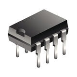
ADC Single SAR 40ksps 8-bit Serial 8-Pin PDIP Tube, TLC549IP, Texas Instruments

The TLC548 and TLC549 are CMOS analog-to-digital converter (ADC) integrated circuits built around an 8-bit switched-capacitor successive-approximation ADC. These devices are designed for serial interface with a microprocessor or peripheral through a 3-state data output and an analog input. The TLC548 and TLC549 use only the input/output clock (I/O CLOCK) input along with the chip select (CS) input for data control. The maximumI/O CLOCK input frequency of the TLC548 is 2.048 MHz, and the I/O CLOCK input frequency of the TLC549 is specified up to 1.1 MHz.  Operation of the TLC548 and the TLC549 is very similar to that of the more complex TLC540 and TLC541 devices; however, the TLC548 and TLC549 provide an on-chip system clock that operates typically at 4 MHz and requires no external components. The on-chip system clock allows internal device operation to proceed independently of serial input/output data timing and permits manipulation of the TLC548 and TLC549 as desired for a wide range of software and hardware requirements. The I/O CLOCK together with the internal system clock allow high-speed data transfer and conversion rates of 45 500 conversions per second for the TLC548, and 40 000 conversions per second for the TLC549. Additional TLC548 and TLC549 features include versatile control logic, an on-chip sample-and-hold circuit that can operate automatically or under microprocessor control, and a high-speed converter with differential high-impedance reference voltage inputs that ease ratiometric conversion, scaling, and circuit isolation from logic and supply noises. Design of the totally switched-capacitor successive-approximation converter circuit allows conversion with a maximum total error of ±0.5 least significant bit (LSB) in less than 17 us. The TLC548C and TLC549C are characterized for operation from 0°C to 70°C. The TLC548I and TLC549I are characterized for operation from -40°C to 85°C.

  • Microprocessor Peripheral or Standalone Operation
  • 8-Bit Resolution A/D Converter
  • Differential Reference Input Voltages
  • Conversion Time. . . 17 us Max
  • Total Access and Conversion Cycles Per Second
    – TLC548 . . . up to 45 500
    – TLC549 . . . up to 40 000
  • On-Chip Software-Controllable Sample-and-Hold Function
  • Total Unadjusted Error . . . ±0.5 LSB Max
  • 4-MHz Typical Internal System Clock
  • Wide Supply Range . . . 3 V to 6 V
  • Low Power Consumption . . . 15 mW Max
  • Ideal for Cost-Effective, High-Performance Applications including Battery-Operated Portable Instrumentation
  • Pinout and Control Signals Compatible With the TLC540 and TLC545 8-Bit A/D Converters and with the TLC1540 10-Bit A/D Converter
  • CMOS Technology


  • Характеристики

    Number_of_analog_inputs

    1

    Digital_supply_support

    No

    Architecture

    SAR

    Resolution

    8 Bit

    Differential_nonlinearity

    0.5 LSB

    Бренд

    Country_of_origin

    Mexico

    Eccn

    EAR99

    Htsn

    8542390001

    Lead_finish

    Gold

    Mounting

    Through Hole

    Pin_count

    8

    Product_dimensions

    9.81 x 6.35 x 4.57 mm

    Schedule_b

    8542390000

    Specifications

    http://www.ti.com/general/docs/lit/getliterature.tsp?genericPartNumber=TLC548&&fileType=pdf

    Operating_supply_volt

    3, 5 V, 6

    Number_of_adcs

    1

    Артикул: TLC549IP

    Описание

    The TLC548 and TLC549 are CMOS analog-to-digital converter (ADC) integrated circuits built around an 8-bit switched-capacitor successive-approximation ADC. These devices are designed for serial interface with a microprocessor or peripheral through a 3-state data output and an analog input. The TLC548 and TLC549 use only the input/output clock (I/O CLOCK) input along with the chip select (CS) input for data control. The maximumI/O CLOCK input frequency of the TLC548 is 2.048 MHz, and the I/O CLOCK input frequency of the TLC549 is specified up to 1.1 MHz.  Operation of the TLC548 and the TLC549 is very similar to that of the more complex TLC540 and TLC541 devices; however, the TLC548 and TLC549 provide an on-chip system clock that operates typically at 4 MHz and requires no external components. The on-chip system clock allows internal device operation to proceed independently of serial input/output data timing and permits manipulation of the TLC548 and TLC549 as desired for a wide range of software and hardware requirements. The I/O CLOCK together with the internal system clock allow high-speed data transfer and conversion rates of 45 500 conversions per second for the TLC548, and 40 000 conversions per second for the TLC549. Additional TLC548 and TLC549 features include versatile control logic, an on-chip sample-and-hold circuit that can operate automatically or under microprocessor control, and a high-speed converter with differential high-impedance reference voltage inputs that ease ratiometric conversion, scaling, and circuit isolation from logic and supply noises. Design of the totally switched-capacitor successive-approximation converter circuit allows conversion with a maximum total error of ±0.5 least significant bit (LSB) in less than 17 us. The TLC548C and TLC549C are characterized for operation from 0°C to 70°C. The TLC548I and TLC549I are characterized for operation from -40°C to 85°C.

  • Microprocessor Peripheral or Standalone Operation
  • 8-Bit Resolution A/D Converter
  • Differential Reference Input Voltages
  • Conversion Time. . . 17 us Max
  • Total Access and Conversion Cycles Per Second
    – TLC548 . . . up to 45 500
    – TLC549 . . . up to 40 000
  • On-Chip Software-Controllable Sample-and-Hold Function
  • Total Unadjusted Error . . . ±0.5 LSB Max
  • 4-MHz Typical Internal System Clock
  • Wide Supply Range . . . 3 V to 6 V
  • Low Power Consumption . . . 15 mW Max
  • Ideal for Cost-Effective, High-Performance Applications including Battery-Operated Portable Instrumentation
  • Pinout and Control Signals Compatible With the TLC540 and TLC545 8-Bit A/D Converters and with the TLC1540 10-Bit A/D Converter
  • CMOS Technology


  • Детали

    Number_of_analog_inputs

    1

    Digital_supply_support

    No

    Architecture

    SAR

    Resolution

    8 Bit

    Differential_nonlinearity

    0.5 LSB

    Бренд

    Country_of_origin

    Mexico

    Eccn

    EAR99

    Htsn

    8542390001

    Lead_finish

    Gold

    Mounting

    Through Hole

    Pin_count

    8

    Product_dimensions

    9.81 x 6.35 x 4.57 mm

    Schedule_b

    8542390000

    Specifications

    http://www.ti.com/general/docs/lit/getliterature.tsp?genericPartNumber=TLC548&&fileType=pdf

    Operating_supply_volt

    3, 5 V, 6

    Number_of_adcs

    1