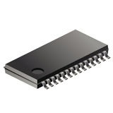
ADC Single Pipelined 35Msps 8-bit Parallel 28-Pin TSSOP T/R, TLV5535IPWRG4Q1, Texas Instruments

The TLV5535 is an 8-bit, 35 MSPS, high-speed A/D converter. It converts the analog input signal into 8-bit binary-coded digital words up to a sampling rate of 35 MHz. All digital inputs and outputs are 3.3 V TTL/CMOS-compatible. The device consumes very little power due to the 3.3-V supply and an innovative single-pipeline architecture implemented in a CMOS process. The user obtains maximum flexibility by setting both bottom and top voltage references from user-supplied voltages. If no external references are available, on-chip references are available for internal and external use. The full-scale range is 1 Vpp up to 1.6 Vpp, depending on the analog supply voltage. If external references are available, the internal references can be disabled independently from the rest of the chip, resulting in an even greater power saving. While usable in a wide variety of applications, the device is specifically suited for the digitizing of high-speed graphics and for interfacing to LCD panels or LCD/DMD projection modules . Other applications include DVD read channel digitization, medical imaging, and communications. This device is suitable for IF sampling of communication systems using sub-Nyquist sampling methods because of its high analog input bandwidth. 

  • Meets AEC-Q100-011 C3A CDM Classification
  • Qualified for Automotive Applications
  • 8-Bit Resolution, 35 MSPS Sampling Analog-to-Digital Converter (ADC)
  • Low Power Consumption: 90 mW Typ Using External References
  • Wide Analog Input Bandwidth: 600 MHz Typ
  • 3.3-V Single-Supply Operation
  • 3.3-V TTL/CMOS-Compatible Digital I/O
  • Internal Bottom and Top Reference Voltages
  • Adjustable Reference Input Range
  • Power-Down (Standby) Mode
  • Separate Power Down for Internal Voltage References
  • Three-State Outputs
  • 28-Pin Thin Shrink SOP (TSSOP) Packages
  • Applications
    • Digital Communications (IF Sampling)
    • High-Speed DSP Front-End (TMS320C6000)
    • Video Processing (Scan Rate/Format Conversion)
    • DVD Read Channel Digitization
  • Характеристики

    Volt_supply_source

    Analog and Digital

    Number_of_analog_inputs

    1

    Sampling_rate

    35 Msps

    Volt_reference

    External, Internal

    Digital_supply_support

    Yes

    Architecture

    Pipelined

    Resolution

    8 Bit

    Typical_power_dissipation

    106 mW

    Differential_nonlinearity

    -1, 1.3 LSB

    Signal_to_noise_ratio

    46.5 dB

    Input_type

    Voltage

    Input_signal_type

    Single-Ended

    Input_volt

    ±0.8 V

    Бренд

    Msl_level

    1

    Country_of_origin

    United States

    Eccn

    EAR99

    Htsn

    8542390001

    Lead_finish

    Gold

    Max_power_dissipation

    139 mW

    Max_processing_temp

    260

    Mounting

    Surface Mount

    Operating_temp

    -40 to 85 °C

    Pin_count

    28

    Product_dimensions

    9.8 x 4.5 x 1.05 mm

    Schedule_b

    8542390000

    Screening_level

    Automotive

    Specifications

    http://www.ti.com/general/docs/lit/getliterature.tsp?genericPartNumber=TLV5535-Q1&&fileType=pdf

    Supplier_package

    TSSOP

    Polarity_of_input_volt

    Bipolar

    Operating_supply_volt

    3, 3.3 V, 3.6

    Number_of_adcs

    1

    Digital_interface_type

    Parallel

    SKU: TLV5535IPWRG4Q1

    Description

    The TLV5535 is an 8-bit, 35 MSPS, high-speed A/D converter. It converts the analog input signal into 8-bit binary-coded digital words up to a sampling rate of 35 MHz. All digital inputs and outputs are 3.3 V TTL/CMOS-compatible. The device consumes very little power due to the 3.3-V supply and an innovative single-pipeline architecture implemented in a CMOS process. The user obtains maximum flexibility by setting both bottom and top voltage references from user-supplied voltages. If no external references are available, on-chip references are available for internal and external use. The full-scale range is 1 Vpp up to 1.6 Vpp, depending on the analog supply voltage. If external references are available, the internal references can be disabled independently from the rest of the chip, resulting in an even greater power saving. While usable in a wide variety of applications, the device is specifically suited for the digitizing of high-speed graphics and for interfacing to LCD panels or LCD/DMD projection modules . Other applications include DVD read channel digitization, medical imaging, and communications. This device is suitable for IF sampling of communication systems using sub-Nyquist sampling methods because of its high analog input bandwidth. 

  • Meets AEC-Q100-011 C3A CDM Classification
  • Qualified for Automotive Applications
  • 8-Bit Resolution, 35 MSPS Sampling Analog-to-Digital Converter (ADC)
  • Low Power Consumption: 90 mW Typ Using External References
  • Wide Analog Input Bandwidth: 600 MHz Typ
  • 3.3-V Single-Supply Operation
  • 3.3-V TTL/CMOS-Compatible Digital I/O
  • Internal Bottom and Top Reference Voltages
  • Adjustable Reference Input Range
  • Power-Down (Standby) Mode
  • Separate Power Down for Internal Voltage References
  • Three-State Outputs
  • 28-Pin Thin Shrink SOP (TSSOP) Packages
  • Applications
    • Digital Communications (IF Sampling)
    • High-Speed DSP Front-End (TMS320C6000)
    • Video Processing (Scan Rate/Format Conversion)
    • DVD Read Channel Digitization
  • Additional information

    Volt_supply_source

    Analog and Digital

    Number_of_analog_inputs

    1

    Sampling_rate

    35 Msps

    Volt_reference

    External, Internal

    Digital_supply_support

    Yes

    Architecture

    Pipelined

    Resolution

    8 Bit

    Typical_power_dissipation

    106 mW

    Differential_nonlinearity

    -1, 1.3 LSB

    Signal_to_noise_ratio

    46.5 dB

    Input_type

    Voltage

    Input_signal_type

    Single-Ended

    Input_volt

    ±0.8 V

    Бренд

    Msl_level

    1

    Country_of_origin

    United States

    Eccn

    EAR99

    Htsn

    8542390001

    Lead_finish

    Gold

    Max_power_dissipation

    139 mW

    Max_processing_temp

    260

    Mounting

    Surface Mount

    Operating_temp

    -40 to 85 °C

    Pin_count

    28

    Product_dimensions

    9.8 x 4.5 x 1.05 mm

    Schedule_b

    8542390000

    Screening_level

    Automotive

    Specifications

    http://www.ti.com/general/docs/lit/getliterature.tsp?genericPartNumber=TLV5535-Q1&&fileType=pdf

    Supplier_package

    TSSOP

    Polarity_of_input_volt

    Bipolar

    Operating_supply_volt

    3, 3.3 V, 3.6

    Number_of_adcs

    1

    Digital_interface_type

    Parallel