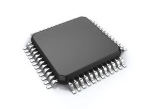
ADC Single Pipelined 210Msps 14-bit Parallel/LVDS 48-Pin VQFN EP T/R, ADS6148IRGZT, Texas Instruments

ADS614X (ADS612X) is a family of 14-bit (12-bit) A/D converters with sampling rates up to 250 MSPS. It combines high dynamic performance and low power consumption in a compact 48 QFN package. This makes it well-suited for multicarrier, wide band-width communications applications.ADS614X/2X has fine gain options that can be used to improve SFDR performance at lower full-scale input ranges. It includes a dc offset correction loop that can be used to cancel the ADC offset. Both DDR LVDS (Double Data Rate) and parallel CMOS digital output interfaces are available. At lower sampling rates, the ADC automatically operates at scaled down power with no loss in performance.It includes internal references while the traditional reference pins and associated decoupling capacitors have been eliminated. Nevertheless, the device can also be driven with an external reference. The device is specified over the industrial temperature range (-40°C to 85°C). 

  • Maximum Sample Rate: 250 MSPS
  • 14-Bit Resolution — ADS614X
  • 12-Bit Resolution — ADS612X
  • 687 mW Total Power Dissipation at 250 MSPS
  • Double Data Rate (DDR) LVDS and Parallel CMOS Output Options
  • Programmable Fine Gain up to 6dB for SNR/SFDR Trade-Off
  • DC Offset Correction
  • Supports Input Clock Amplitude Down to 400 mVPP Differential
  • Internal and External Reference Support
  • 48-QFN Package (7mm × 7mm)
  • Pin Compatible with ADS5547 Family
  • APPLICATIONS
    • Multicarrier, Wide Band-Width Communications
    • Wireless Multi-carrier Communications Infrastructure
    • Software Defined Radio
    • Power Amplifier Linearization
    • 802.16d/e
    • Test and Measurement Instrumentation
    • High Definition Video
    • Medical Imaging
    • Radar Systems
  • Характеристики

    Volt_supply_source

    Analog and Digital

    Number_of_analog_inputs

    1

    Sampling_rate

    210 Msps

    Volt_reference

    External, Internal

    Digital_supply_support

    Yes

    Architecture

    Pipelined

    Resolution

    14 Bit

    Differential_nonlinearity

    0.4 LSB

    Signal_to_noise_ratio

    73.4 dBFS

    Input_type

    Voltage

    Input_signal_type

    Differential

    Input_volt

    2 Vp-p

    Бренд

    Msl_level

    3

    Country_of_origin

    United States

    Eccn

    3A991.C.3

    Htsn

    8542390001

    Lead_finish

    Gold

    Max_power_dissipation

    687 mW

    Max_processing_temp

    260

    Mounting

    Surface Mount

    Operating_temp

    -40 to 85 °C

    Pin_count

    48

    Product_dimensions

    7 x 7 x 0.9 mm

    Schedule_b

    8542390000

    Screening_level

    Industrial

    Specifications

    http://www.ti.com/general/docs/lit/getliterature.tsp?genericPartNumber=ADS6148&&fileType=pdf

    Supplier_package

    VQFN EP

    Operating_supply_volt

    3, 3.3 V, 3.6

    Number_of_adcs

    1

    Digital_interface_type

    LVDS, Parallel

    SKU: ADS6148IRGZT

    Description

    ADS614X (ADS612X) is a family of 14-bit (12-bit) A/D converters with sampling rates up to 250 MSPS. It combines high dynamic performance and low power consumption in a compact 48 QFN package. This makes it well-suited for multicarrier, wide band-width communications applications.ADS614X/2X has fine gain options that can be used to improve SFDR performance at lower full-scale input ranges. It includes a dc offset correction loop that can be used to cancel the ADC offset. Both DDR LVDS (Double Data Rate) and parallel CMOS digital output interfaces are available. At lower sampling rates, the ADC automatically operates at scaled down power with no loss in performance.It includes internal references while the traditional reference pins and associated decoupling capacitors have been eliminated. Nevertheless, the device can also be driven with an external reference. The device is specified over the industrial temperature range (-40°C to 85°C). 

  • Maximum Sample Rate: 250 MSPS
  • 14-Bit Resolution — ADS614X
  • 12-Bit Resolution — ADS612X
  • 687 mW Total Power Dissipation at 250 MSPS
  • Double Data Rate (DDR) LVDS and Parallel CMOS Output Options
  • Programmable Fine Gain up to 6dB for SNR/SFDR Trade-Off
  • DC Offset Correction
  • Supports Input Clock Amplitude Down to 400 mVPP Differential
  • Internal and External Reference Support
  • 48-QFN Package (7mm × 7mm)
  • Pin Compatible with ADS5547 Family
  • APPLICATIONS
    • Multicarrier, Wide Band-Width Communications
    • Wireless Multi-carrier Communications Infrastructure
    • Software Defined Radio
    • Power Amplifier Linearization
    • 802.16d/e
    • Test and Measurement Instrumentation
    • High Definition Video
    • Medical Imaging
    • Radar Systems
  • Additional information

    Volt_supply_source

    Analog and Digital

    Number_of_analog_inputs

    1

    Sampling_rate

    210 Msps

    Volt_reference

    External, Internal

    Digital_supply_support

    Yes

    Architecture

    Pipelined

    Resolution

    14 Bit

    Differential_nonlinearity

    0.4 LSB

    Signal_to_noise_ratio

    73.4 dBFS

    Input_type

    Voltage

    Input_signal_type

    Differential

    Input_volt

    2 Vp-p

    Бренд

    Msl_level

    3

    Country_of_origin

    United States

    Eccn

    3A991.C.3

    Htsn

    8542390001

    Lead_finish

    Gold

    Max_power_dissipation

    687 mW

    Max_processing_temp

    260

    Mounting

    Surface Mount

    Operating_temp

    -40 to 85 °C

    Pin_count

    48

    Product_dimensions

    7 x 7 x 0.9 mm

    Schedule_b

    8542390000

    Screening_level

    Industrial

    Specifications

    http://www.ti.com/general/docs/lit/getliterature.tsp?genericPartNumber=ADS6148&&fileType=pdf

    Supplier_package

    VQFN EP

    Operating_supply_volt

    3, 3.3 V, 3.6

    Number_of_adcs

    1

    Digital_interface_type

    LVDS, Parallel