ADC Single Multi-Slope 40sps 15-bit+Sign Parallel 44-Pin PLCC Tube, TC850ILW, Microchip

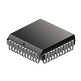
The TC850 is a monolithic CMOS A/D converter (ADC) with resolution of 15-bits plus sign. It combines a chopper-stabilized buffer and integrator with a unique multiple-slope integration technique that increases conversion speed. The result is 16 times improvement in speed over previous 15-bit, monolithic integrating ADCs (from 2.5 conversions per second up to 40 per second). Faster conversion speed is especially welcome in systems with human interface, such as digital scales. The TC850 incorporates an ADC and a µP-compatible digital interface. Only a voltage reference and a few, noncritical, passive components are required to form a complete 15-bit plus sign ADC. CMOS processing provides the TC850 with high-impedance, differential inputs. Input bias current is typically only 30 pA, permitting direct interface to sensors. Input sensitivity of 100 µV per Least Significant bit (LSb) eliminates the need for precision external amplifiers. The internal amplifiers are auto-zeroed, ensuring a zero digital output, with 0V analog input. Zero adjustment potentiometers or calibrations are not required. The TC850 outputs data on an 8-bit, 3-state bus. Digital inputs are CMOS compatible while outputs are TTL/ CMOS compatible. Chip-enable and byte-select inputs, combined with an end-of-conversion output, ensures easy interfacing to a wide variety of microprocessors. Conversions can be performed continuously or on command. In Continuous mode, data is read as three consecutive bytes and manipulation of address lines is not required. Operating from ±5V supplies, the TC850 dissipates only 20 mO. The TC850 is packaged in a 40-pin plastic or ceramic dual-in-line package (DIPs) and in a 44-pin plastic leaded chip carrier (PLCC), surface-mount package.

  • 15-bit Resolution Plus Sign Bit
  • Up to 40 Conversions per Second
  • Integrating ADC Technique: – Monotonic – High Noise Immunity – Auto-Zeroed Amplifiers Eliminate Offset Trimming
  • Wide Dynamic Range: 96 dB
  • Low Input Bias Current: 30 pA
  • Low Input Noise: 30 µVP-P
  • Sensitivity: 100 µV
  • Flexible Operational Control
  • Continuous or On Demand Conversions
  • Data Valid Output
  • Bus Compatible, 3-State Data Outputs: – 8-Bit Data Bus – Simple µP Interface – Two Chip Enables – Read ADC Result Like Memory
  • ± 5V Power Supply Operation: 20 mO
  • 40-Pin Dual-in-Line or 44-Pin PLCC Packages
Характеристики

Volt_supply_source

Dual

Number_of_analog_inputs

1

Sampling_rate

40 sps

Volt_reference

External

Digital_supply_support

No

Architecture

Multi-Slope

Resolution

15+Sign Bit

Differential_nonlinearity

0.5 LSB

Input_type

Voltage

Input_signal_type

Differential

Input_volt

3.277 V

Бренд

Msl_level

1, 3

Country_of_origin

China

Eccn

EAR99

Htsn

8542390001

Lead_finish

Matte Tin

Max_power_dissipation

1230 mW

Max_processing_temp

260

Mounting

Surface Mount

Operating_temp

-25 to 85 °C

Pin_count

44

Product_dimensions

16.59 x 16.59 x 3.87 mm

Schedule_b

8542390000

Specifications

https://4donline.ihs.com/images/VipMasterIC/IC/MCHP/MCHPS04171/MCHPS04171-1.pdf?hkey=52A5661711E402568146F3353EA87419

Supplier_package

PLCC

Number_of_adc_channels

1

Polarity_of_input_volt

Unipolar

Operating_supply_volt

±5 V

Number_of_adcs

1

Digital_interface_type

Parallel

Артикул: TC850ILW

Описание

The TC850 is a monolithic CMOS A/D converter (ADC) with resolution of 15-bits plus sign. It combines a chopper-stabilized buffer and integrator with a unique multiple-slope integration technique that increases conversion speed. The result is 16 times improvement in speed over previous 15-bit, monolithic integrating ADCs (from 2.5 conversions per second up to 40 per second). Faster conversion speed is especially welcome in systems with human interface, such as digital scales. The TC850 incorporates an ADC and a µP-compatible digital interface. Only a voltage reference and a few, noncritical, passive components are required to form a complete 15-bit plus sign ADC. CMOS processing provides the TC850 with high-impedance, differential inputs. Input bias current is typically only 30 pA, permitting direct interface to sensors. Input sensitivity of 100 µV per Least Significant bit (LSb) eliminates the need for precision external amplifiers. The internal amplifiers are auto-zeroed, ensuring a zero digital output, with 0V analog input. Zero adjustment potentiometers or calibrations are not required. The TC850 outputs data on an 8-bit, 3-state bus. Digital inputs are CMOS compatible while outputs are TTL/ CMOS compatible. Chip-enable and byte-select inputs, combined with an end-of-conversion output, ensures easy interfacing to a wide variety of microprocessors. Conversions can be performed continuously or on command. In Continuous mode, data is read as three consecutive bytes and manipulation of address lines is not required. Operating from ±5V supplies, the TC850 dissipates only 20 mO. The TC850 is packaged in a 40-pin plastic or ceramic dual-in-line package (DIPs) and in a 44-pin plastic leaded chip carrier (PLCC), surface-mount package.

  • 15-bit Resolution Plus Sign Bit
  • Up to 40 Conversions per Second
  • Integrating ADC Technique: – Monotonic – High Noise Immunity – Auto-Zeroed Amplifiers Eliminate Offset Trimming
  • Wide Dynamic Range: 96 dB
  • Low Input Bias Current: 30 pA
  • Low Input Noise: 30 µVP-P
  • Sensitivity: 100 µV
  • Flexible Operational Control
  • Continuous or On Demand Conversions
  • Data Valid Output
  • Bus Compatible, 3-State Data Outputs: – 8-Bit Data Bus – Simple µP Interface – Two Chip Enables – Read ADC Result Like Memory
  • ± 5V Power Supply Operation: 20 mO
  • 40-Pin Dual-in-Line or 44-Pin PLCC Packages
Детали

Volt_supply_source

Dual

Number_of_analog_inputs

1

Sampling_rate

40 sps

Volt_reference

External

Digital_supply_support

No

Architecture

Multi-Slope

Resolution

15+Sign Bit

Differential_nonlinearity

0.5 LSB

Input_type

Voltage

Input_signal_type

Differential

Input_volt

3.277 V

Бренд

Msl_level

1, 3

Country_of_origin

China

Eccn

EAR99

Htsn

8542390001

Lead_finish

Matte Tin

Max_power_dissipation

1230 mW

Max_processing_temp

260

Mounting

Surface Mount

Operating_temp

-25 to 85 °C

Pin_count

44

Product_dimensions

16.59 x 16.59 x 3.87 mm

Schedule_b

8542390000

Specifications

https://4donline.ihs.com/images/VipMasterIC/IC/MCHP/MCHPS04171/MCHPS04171-1.pdf?hkey=52A5661711E402568146F3353EA87419

Supplier_package

PLCC

Number_of_adc_channels

1

Polarity_of_input_volt

Unipolar

Operating_supply_volt

±5 V

Number_of_adcs

1

Digital_interface_type

Parallel