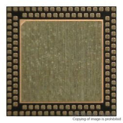
ADC Pipelined 1-CH 200Msps 12-bit Parallel CMOS/Serial DDR LVDS 124-Pin VTLA T/R, MCP37D10T-200I/TL, Microchip

The MCP37210-200 is a single-channel 200 Msps 12-bit pipelined ADC, with built-in high-order digital decimation filters, Noise-Shaping Re-quantizer (NSR), gain and offset adjustment.The MCP37D10-200 is also a single-channel 200 Msps 12-bit pipelined ADC, with built-in digital down-conversion in addition to the features offered by the MCP37210-200.Both devices feature harmonic distortion correction and DAC noise cancellation that enables high-performance specifications with SNR of 67 dBFS (typical) and SFDR of 96 dBc (typical).The output decimation filter option improves SNR performance up to 73.5 dBFS with the 64x decimation setting.The digital down-conversion option in the MCP37D10-200 can be utilized with the decimation and quadrature output (I and Q data) options, and offers great flexibility in various digital communication system designs, including cellular base-stations and narrow-band communication systems.These A/D converters exhibit industry-leading low-power performance with only 338 mW operation, while using the LVDS output interface at 200 Msps. This superior low-power operation, coupled with high dynamic performance, makes these devices ideal for portable high-frequency instrumentation, sonar, radar, and high-speed data acquisition systems.These devices also include various features designed to maximize flexibility in the user"s applications and minimize system cost, such as a programmable PLL clock, output data rate control and phase alignment, and programmable digital pattern generation. The device"s operational modes and feature sets are configured by setting up the user-programmable internal registers. The device samples the analog input on the rising edge of the clock. The digital output code is available after 23 clock cycles of data latency. Latency will increase if any of the digital signal post-processing (DSPP) options are enabled.

  • Sample Rates: 200 Msps
  • Signal-to-Noise Ratio (SNR) with fIN = 15 MHz and -1 dBFS:
    • 67 dBFS (typical) at 200 Msps
  • Spurious-Free Dynamic Range (SFDR) with fIN = 15 MHz and -1 dBFS:
    • 96 dBc (typical) at 200 Msps
  • Power Dissipation with LVDS Digital I/O:
    • 338 mW at 200 Msps
  • Power Dissipation with CMOS Digital I/O:
    • 306 mW at 200 Msps, output clock = 100 MHz
  • Power Dissipation Excluding Digital I/O:
    • 257 mW at 200 Msps
  • Power-Saving Modes:
    • 80 mW during Standby
    • 33 mW during Shutdown
  • Supply Voltage:
    • Digital Section: 1.2V, 1.8V
    • Analog Section: 1.2V, 1.8V
  • Selectable Full-Scale Input Range: up to 1.8 VP-P
  • Analog Input Bandwidth: 650 MHz
  • Output Interface:
    • Parallel CMOS, DDR LVDS
  • Output Data Format:
    • Two"s complement or offset binary
  • Optional Output Data Randomizer
  • Digital Signal Post-Processing (DSPP) Options:
    • Decimation filters for improved SNR
    • Offset and Gain adjustment
    • Noise-Shaping Requantizer (NSR)
    • Digital Down-Conversion (DDC) with I/Q or fS/8 output (MCP37D10-200)
  • Built-In ADC Linearity Calibration Algorithms:
    • Harmonic Distortion Correction (HDC)
    • DAC Noise Cancellation (DNC)
    • Dynamic Element Matching (DEM)
    • Flash Error Calibration
  • Serial Peripheral Interface (SPI)
  • Package Options:
    • VTLA-124 (9 mm x 9 mm x 0.9 mm)
    • TFBGA-121 (8 mm x 8 mm x 1.08 mm)
  • No external reference decoupling capacitor required for TFBGA Package
  • Industrial Temperature Range: -40°C to +85°C
  • Tape and Reel Packaging

Характеристики

Volt_supply_source

Analog, Digital

Eccn

EAR99

Sampling_rate

200 Msps

Volt_reference

Internal

Resolution

12 Bit

Integral_nonlinearity_error

±0.375(Typ) LSB

Typical_power_dissipation

360 mW

Differential_nonlinearity

0.1(Typ) LSB

Signal_to_noise_ratio

67 dBFS

Input_type

Voltage

Input_signal_type

Differential, Single-Ended

Input_volt

1.8 V

Бренд

Msl_level

1

Country_of_origin

China

Number_of_analog_inputs

1

Lead_finish

Gold Over Nickel Palladium

Htsn

8542390001

Max_processing_temp

260

Mounting

Surface Mount

Operating_temp

-40 to 85 °C

Pin_count

124

Product_dimensions

9 x 9 x 0.85(Max)

Schedule_b

8542390000

Screening_level

Industrial

Specifications

https://4donline.ihs.com/images/VipMasterIC/IC/MCHP/MCHP-S-A0001788602/MCHP-S-A0001788602-1.pdf?hkey=52A5661711E402568146F3353EA87419

Supplier_package

VTLA

Number_of_adc_channels

1

Polarity_of_input_volt

Bipolar, Unipolar

Operating_supply_volt

1.14, 1.26, 1.71 V, 1.89

Number_of_adcs

1

Digital_interface_type

Parallel CMOS, Serial DDR LVDS

Артикул: MCP37D10T-200I/TL

Описание

The MCP37210-200 is a single-channel 200 Msps 12-bit pipelined ADC, with built-in high-order digital decimation filters, Noise-Shaping Re-quantizer (NSR), gain and offset adjustment.The MCP37D10-200 is also a single-channel 200 Msps 12-bit pipelined ADC, with built-in digital down-conversion in addition to the features offered by the MCP37210-200.Both devices feature harmonic distortion correction and DAC noise cancellation that enables high-performance specifications with SNR of 67 dBFS (typical) and SFDR of 96 dBc (typical).The output decimation filter option improves SNR performance up to 73.5 dBFS with the 64x decimation setting.The digital down-conversion option in the MCP37D10-200 can be utilized with the decimation and quadrature output (I and Q data) options, and offers great flexibility in various digital communication system designs, including cellular base-stations and narrow-band communication systems.These A/D converters exhibit industry-leading low-power performance with only 338 mW operation, while using the LVDS output interface at 200 Msps. This superior low-power operation, coupled with high dynamic performance, makes these devices ideal for portable high-frequency instrumentation, sonar, radar, and high-speed data acquisition systems.These devices also include various features designed to maximize flexibility in the user"s applications and minimize system cost, such as a programmable PLL clock, output data rate control and phase alignment, and programmable digital pattern generation. The device"s operational modes and feature sets are configured by setting up the user-programmable internal registers. The device samples the analog input on the rising edge of the clock. The digital output code is available after 23 clock cycles of data latency. Latency will increase if any of the digital signal post-processing (DSPP) options are enabled.

  • Sample Rates: 200 Msps
  • Signal-to-Noise Ratio (SNR) with fIN = 15 MHz and -1 dBFS:
    • 67 dBFS (typical) at 200 Msps
  • Spurious-Free Dynamic Range (SFDR) with fIN = 15 MHz and -1 dBFS:
    • 96 dBc (typical) at 200 Msps
  • Power Dissipation with LVDS Digital I/O:
    • 338 mW at 200 Msps
  • Power Dissipation with CMOS Digital I/O:
    • 306 mW at 200 Msps, output clock = 100 MHz
  • Power Dissipation Excluding Digital I/O:
    • 257 mW at 200 Msps
  • Power-Saving Modes:
    • 80 mW during Standby
    • 33 mW during Shutdown
  • Supply Voltage:
    • Digital Section: 1.2V, 1.8V
    • Analog Section: 1.2V, 1.8V
  • Selectable Full-Scale Input Range: up to 1.8 VP-P
  • Analog Input Bandwidth: 650 MHz
  • Output Interface:
    • Parallel CMOS, DDR LVDS
  • Output Data Format:
    • Two"s complement or offset binary
  • Optional Output Data Randomizer
  • Digital Signal Post-Processing (DSPP) Options:
    • Decimation filters for improved SNR
    • Offset and Gain adjustment
    • Noise-Shaping Requantizer (NSR)
    • Digital Down-Conversion (DDC) with I/Q or fS/8 output (MCP37D10-200)
  • Built-In ADC Linearity Calibration Algorithms:
    • Harmonic Distortion Correction (HDC)
    • DAC Noise Cancellation (DNC)
    • Dynamic Element Matching (DEM)
    • Flash Error Calibration
  • Serial Peripheral Interface (SPI)
  • Package Options:
    • VTLA-124 (9 mm x 9 mm x 0.9 mm)
    • TFBGA-121 (8 mm x 8 mm x 1.08 mm)
  • No external reference decoupling capacitor required for TFBGA Package
  • Industrial Temperature Range: -40°C to +85°C
  • Tape and Reel Packaging

Детали

Volt_supply_source

Analog, Digital

Eccn

EAR99

Sampling_rate

200 Msps

Volt_reference

Internal

Resolution

12 Bit

Integral_nonlinearity_error

±0.375(Typ) LSB

Typical_power_dissipation

360 mW

Differential_nonlinearity

0.1(Typ) LSB

Signal_to_noise_ratio

67 dBFS

Input_type

Voltage

Input_signal_type

Differential, Single-Ended

Input_volt

1.8 V

Бренд

Msl_level

1

Country_of_origin

China

Number_of_analog_inputs

1

Lead_finish

Gold Over Nickel Palladium

Htsn

8542390001

Max_processing_temp

260

Mounting

Surface Mount

Operating_temp

-40 to 85 °C

Pin_count

124

Product_dimensions

9 x 9 x 0.85(Max)

Schedule_b

8542390000

Screening_level

Industrial

Specifications

https://4donline.ihs.com/images/VipMasterIC/IC/MCHP/MCHP-S-A0001788602/MCHP-S-A0001788602-1.pdf?hkey=52A5661711E402568146F3353EA87419

Supplier_package

VTLA

Number_of_adc_channels

1

Polarity_of_input_volt

Bipolar, Unipolar

Operating_supply_volt

1.14, 1.26, 1.71 V, 1.89

Number_of_adcs

1

Digital_interface_type

Parallel CMOS, Serial DDR LVDS