Описание
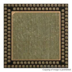
The MCP37210-200 is a single-channel 200 Msps 12-bit pipelined ADC, with built-in high-order digital decimation filters, Noise-Shaping re-quantizer (NSR), gain and offset adjustment. These devices feature harmonic distortion correction and DAC noise cancellation that enables highperformance specifications with SNR of 67 dBFS (typical) and SFDR of 96 dBc (typical). The output decimation filter option improves SNR performance up to 73.5 dBFS with the 64x decimation setting. The NSR feature reshapes the quantization noise level so that most of the noise power is pushed outside the frequency band of interest. As a result, SNR is improved within a selected frequency band of interest, while SFDR is not affected. These A/D converters exhibit industry-leading low-power performance with only 338 mW operation, while using the LVDS output interface at 200 Msps. This superior low-power operation, coupled with high dynamic performance, makes these devices ideal for portable high-frequency instrumentation, sonar, radar, and high-speed data acquisition systems. The device"s operational modes and feature sets are configured by setting up the user-programmable internal registers. The device samples the analog input on the rising edge of the clock. The digital output code is available after 23 clock cycles of data latency. Latency will increase if any of the digital signal post-processing (DSPP) options are enabled. The differential full-scale analog input range is programmable up to 1.8 VP-P. The ADC output data can be coded in two"s complement or offset binary representation, with or without the data randomizer option. The output data is available with a full-rate CMOS or Double-Data-Rate (DDR) LVDS interface. The device is available in Pb-free VTLA-124 and TFBGA-121 packages. The device operates over the commercial temperature range of -40°C to +85°C.
- Sample Rates: 200 Msps
- Signal-to-Noise Ratio (SNR) with fIN = 15 MHz and -1 dBFS:
- 67 dBFS (typical) at 200 Msps
- Spurious-Free Dynamic Range (SFDR) with fIN = 15 MHz and -1 dBFS:
- 96 dBc (typical) at 200 Msps
- Power Dissipation with LVDS Digital I/O:
- 337 mW at 200 Msps
- Power Dissipation with CMOS Digital I/O:
- 304 mW at 200 Msps, output clock = 100 MHz
- Power Dissipation Excluding Digital I/O:
- 256 mW at 200 Msps
- Power-Saving Modes:
- 89 mW during Standby
- 24 mW during Shutdown
- Supply Voltage:
- Digital Section: 1.2V, 1.8V
- Analog Section: 1.2V, 1.8V
- Selectable Full-Scale Input Range: up to 1.8 VP-P
- Analog Input Bandwidth: 650 MHz
- Output Interface:
- Parallel CMOS, DDR LVDS
- Output Data Format:
- Two"s complement or offset binary
- Optional Output Data Randomizer
- Digital Signal Post-Processing (DSPP) Options:
- Decimation filters for improved SNR
- Offset and Gain adjustment
- Noise-Shaping Requantizer (NSR)
- Digital Down-Conversion (DDC) with I/Q or fS/8 output (MCP37D10-200)
- Built-In ADC Linearity Calibration Algorithms:
- Harmonic Distortion Correction (HDC)
- DAC Noise Cancellation (DNC)
- Dynamic Element Matching (DEM)
- Flash Error Calibration
- Serial Peripheral Interface (SPI)
- Package Options:
- VTLA-124 (9 mm x 9 mm x 0.9 mm)
- TFBGA-121 (8 mm x 8 mm)
- No external reference decoupling capacitor required for TFBGA Package
- Industrial Temperature Range: -40°C to +85°C
- Tape and Reel Packaging


