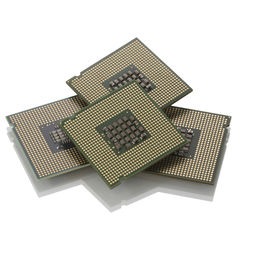
ADC Octal Pipelined 50Msps 12-bit Serial 144-Pin CT-BGA, MAX19527EXE+, Maxim Integrated

The MAX19527 is an octal, 12-bit analog-to-digital converter (ADC), optimized for the low-power and high-dynamic performance requirements of medical imaging instrumentation and digital communications applications. The device operates from a single 1.8V supply and consumes 440mW (55mW per channel), while providing a 69dBFS signal-to-noise ratio (SNR) at a 5.3MHz input frequency. In addition to low operating power, the device features programmable power management for idle states and reduced-channel operation. An internal 1.25V precision bandgap reference sets the full-scale range of the ADC to 1.5VP-P. A flexible reference structure allows the use of an external reference for applications requiring greater gain accuracy or a different input voltage range. A programmable common-mode voltage reference output is provided to enable DC-coupled input applications. Various adjustments and feature selections are available through programmable registers that are accessed through the 3-wire serial peripheral interface (SPI). A flexible clock input circuit allows for a single-ended, logic-level clock or a differential clock signal. An on-chip PLL generates the multiplied (6x) clock required for the serial LVDS digital outputs. The serial LVDS output provides programmable test patterns for data timing alignment and output drivers with programmable current drive and programmable internal termination. The device is available in a small, 10mm x 10mm x 1.2mm, 144-lead thin chip ball grid array (CTBGA) package and is specified for the extended industrial (-40°C to +85°C) temperature range.

  • Ultra-Low-Power Operation
    • 55mW per Channel at 50Msps
  • Single 1.8V Power Supply
  • Excellent Dynamic Performance
    • 69dBFS SNR at 5.3MHz
    • 140dBc/Hz Near-Carrier SNR at 1kHz Offset from a 5.3MHz Tone
    • 84dBc SFDR at 5.3MHz
    • 90dB Channel Isolation at 5.3MHz
  • User-Programmable Adjustment and Feature Selection through an SPI Interface
  • Serial LVDS Outputs with Programmable Current Drive and Internal Termination
  • Programmable Power Management
  • Internal or External Reference Operation
  • Single-Ended or Differential Clock Input
  • Programmable Output Data Format
  • Built-In Output Data Test Patterns
  • Small, 10mm x 10mm, 144-Lead CTBGA Package
  • Evaluation Kit Available (Order MAX19527EVKIT+)
  • Характеристики

    Volt_supply_source

    Single

    Number_of_analog_inputs

    8

    Sampling_rate

    50 Msps

    Volt_reference

    External, Internal

    Digital_supply_support

    No

    Architecture

    Pipelined

    Resolution

    12 Bit

    Typical_power_dissipation

    440 mW

    Differential_nonlinearity

    1 LSB

    Signal_to_noise_ratio

    68.5 dB

    Input_type

    Voltage

    Input_signal_type

    Differential

    Input_volt

    1.5 Vp-p

    Бренд

    Country_of_origin

    United States

    Eccn

    EAR99

    Htsn

    8542390001

    Max_processing_temp

    260, 300

    Mounting

    Surface Mount

    Operating_temp

    -40 to 85 °C

    Pin_count

    144

    Product_dimensions

    10 x 10 x 0.76 mm

    Schedule_b

    8542390000

    Screening_level

    Extended Industrial

    Specifications

    https://4donline.ihs.com/images/VipMasterIC/IC/MAXM/MAXMS10517/MAXMS10517-1.pdf?hkey=52A5661711E402568146F3353EA87419

    Supplier_package

    CTBGA

    Number_of_adc_channels

    8

    Operating_supply_volt

    1.7, 1.8 V, 1.9

    Number_of_adcs

    8

    Digital_interface_type

    LVDS, Serial

    Артикул: MAX19527EXE+

    Описание

    The MAX19527 is an octal, 12-bit analog-to-digital converter (ADC), optimized for the low-power and high-dynamic performance requirements of medical imaging instrumentation and digital communications applications. The device operates from a single 1.8V supply and consumes 440mW (55mW per channel), while providing a 69dBFS signal-to-noise ratio (SNR) at a 5.3MHz input frequency. In addition to low operating power, the device features programmable power management for idle states and reduced-channel operation. An internal 1.25V precision bandgap reference sets the full-scale range of the ADC to 1.5VP-P. A flexible reference structure allows the use of an external reference for applications requiring greater gain accuracy or a different input voltage range. A programmable common-mode voltage reference output is provided to enable DC-coupled input applications. Various adjustments and feature selections are available through programmable registers that are accessed through the 3-wire serial peripheral interface (SPI). A flexible clock input circuit allows for a single-ended, logic-level clock or a differential clock signal. An on-chip PLL generates the multiplied (6x) clock required for the serial LVDS digital outputs. The serial LVDS output provides programmable test patterns for data timing alignment and output drivers with programmable current drive and programmable internal termination. The device is available in a small, 10mm x 10mm x 1.2mm, 144-lead thin chip ball grid array (CTBGA) package and is specified for the extended industrial (-40°C to +85°C) temperature range.

    • Ultra-Low-Power Operation
      • 55mW per Channel at 50Msps
    • Single 1.8V Power Supply
    • Excellent Dynamic Performance
      • 69dBFS SNR at 5.3MHz
      • 140dBc/Hz Near-Carrier SNR at 1kHz Offset from a 5.3MHz Tone
      • 84dBc SFDR at 5.3MHz
      • 90dB Channel Isolation at 5.3MHz
  • User-Programmable Adjustment and Feature Selection through an SPI Interface
  • Serial LVDS Outputs with Programmable Current Drive and Internal Termination
  • Programmable Power Management
  • Internal or External Reference Operation
  • Single-Ended or Differential Clock Input
  • Programmable Output Data Format
  • Built-In Output Data Test Patterns
  • Small, 10mm x 10mm, 144-Lead CTBGA Package
  • Evaluation Kit Available (Order MAX19527EVKIT+)
  • Детали

    Volt_supply_source

    Single

    Number_of_analog_inputs

    8

    Sampling_rate

    50 Msps

    Volt_reference

    External, Internal

    Digital_supply_support

    No

    Architecture

    Pipelined

    Resolution

    12 Bit

    Typical_power_dissipation

    440 mW

    Differential_nonlinearity

    1 LSB

    Signal_to_noise_ratio

    68.5 dB

    Input_type

    Voltage

    Input_signal_type

    Differential

    Input_volt

    1.5 Vp-p

    Бренд

    Country_of_origin

    United States

    Eccn

    EAR99

    Htsn

    8542390001

    Max_processing_temp

    260, 300

    Mounting

    Surface Mount

    Operating_temp

    -40 to 85 °C

    Pin_count

    144

    Product_dimensions

    10 x 10 x 0.76 mm

    Schedule_b

    8542390000

    Screening_level

    Extended Industrial

    Specifications

    https://4donline.ihs.com/images/VipMasterIC/IC/MAXM/MAXMS10517/MAXMS10517-1.pdf?hkey=52A5661711E402568146F3353EA87419

    Supplier_package

    CTBGA

    Number_of_adc_channels

    8

    Operating_supply_volt

    1.7, 1.8 V, 1.9

    Number_of_adcs

    8

    Digital_interface_type

    LVDS, Serial