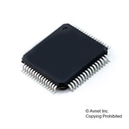
ADC Hex SAR 670ksps 14-bit Parallel/Serial 64-Pin LQFP Tray, ADS8557IPM, Texas Instruments

The ADS8556/7/8 contain six low-power, 16-, 14-, or 12-bit, successive approximation register (SAR) based analog-to-digital converters (ADCs) with true bipolar inputs. Each channel contains a sample-and-hold circuit that allows simultaneous high-speed multi-channel signal acquisition.The ADS8556/7/8 support data rates of up to 730kSPS in parallel interface mode or up to 500kSPS if the serial interface is used. The bus width of the parallel interface can be set to eight or 16 bits. In serial mode, up to three output channels can be activated.The ADS8556/7/8 is specified over the full industrial temperature range of –40°C to +125°C and is available in an LQFP-64 package.

  • Family of 16-, 14-, 12-Bit, Pin- and Software-Compatible ADCs
  • Six SAR ADCs Grouped in Three Pairs
  • Maximum Data Rate Per Channel with Internal Conversion Clock and Reference:
    ADS8556: 630kSPS (PAR) or 450kSPS (SER)
    ADS8557: 670kSPS (PAR) or 470kSPS (SER)
    ADS8558: 730kSPS (PAR) or 500kSPS (SER)
  • Maximum Data Rate with External Conversion Clock and Reference:
    800kSPS (PAR) or 530kSPS (SER)
  • Pin-Selectable or Programmable Input Voltage Ranges: Up to ±12V
  • Excellent Signal-to-Noise Performance:
    91.5dB (ADS8556)
    85dB (ADS8557)
    73.9dB (ADS8558)
  • Programmable and Buffered Internal Reference: 0.5V to 2.5V and 0.5V to 3.0V
  • Comprehensive Power-Down Modes:
    Deep Power-Down (Standby Mode)
    Partial Power-Down
    Auto-Nap Power-Down
  • Selectable Parallel or Serial Interface
  • Operating Temperature Range:
    –40°C to +125°C
  • LQFP-64 Package
  • Характеристики

    Volt_supply_source

    Dual

    Number_of_analog_inputs

    6

    Sampling_rate

    670 ksps

    Volt_reference

    External, Internal

    Digital_supply_support

    No

    Architecture

    SAR

    Resolution

    14 Bit

    Typical_power_dissipation

    253.2 mW

    Differential_nonlinearity

    1 LSB

    Signal_to_noise_ratio

    85 dB

    Input_type

    Voltage

    Input_signal_type

    Single-Ended

    Input_volt

    ±12 V

    Бренд

    Msl_level

    3

    Country_of_origin

    Taiwan

    Eccn

    EAR99

    Htsn

    8542390001

    Lead_finish

    Gold

    Max_power_dissipation

    303 mW

    Max_processing_temp

    260

    Mounting

    Surface Mount

    Operating_temp

    -40 to 125 °C

    Pin_count

    64

    Product_dimensions

    10 x 10 x 1.4 mm

    Schedule_b

    8542390000

    Screening_level

    Industrial

    Specifications

    http://www.ti.com/general/docs/lit/getliterature.tsp?genericPartNumber=ADS8557&&fileType=pdf

    Supplier_package

    LQFP

    Polarity_of_input_volt

    Bipolar

    Operating_supply_volt

    ±10/5 V, ±16.5/5.5

    Number_of_adcs

    6

    Digital_interface_type

    Parallel, Serial

    Артикул: ADS8557IPM

    Описание

    The ADS8556/7/8 contain six low-power, 16-, 14-, or 12-bit, successive approximation register (SAR) based analog-to-digital converters (ADCs) with true bipolar inputs. Each channel contains a sample-and-hold circuit that allows simultaneous high-speed multi-channel signal acquisition.The ADS8556/7/8 support data rates of up to 730kSPS in parallel interface mode or up to 500kSPS if the serial interface is used. The bus width of the parallel interface can be set to eight or 16 bits. In serial mode, up to three output channels can be activated.The ADS8556/7/8 is specified over the full industrial temperature range of –40°C to +125°C and is available in an LQFP-64 package.

  • Family of 16-, 14-, 12-Bit, Pin- and Software-Compatible ADCs
  • Six SAR ADCs Grouped in Three Pairs
  • Maximum Data Rate Per Channel with Internal Conversion Clock and Reference:
    ADS8556: 630kSPS (PAR) or 450kSPS (SER)
    ADS8557: 670kSPS (PAR) or 470kSPS (SER)
    ADS8558: 730kSPS (PAR) or 500kSPS (SER)
  • Maximum Data Rate with External Conversion Clock and Reference:
    800kSPS (PAR) or 530kSPS (SER)
  • Pin-Selectable or Programmable Input Voltage Ranges: Up to ±12V
  • Excellent Signal-to-Noise Performance:
    91.5dB (ADS8556)
    85dB (ADS8557)
    73.9dB (ADS8558)
  • Programmable and Buffered Internal Reference: 0.5V to 2.5V and 0.5V to 3.0V
  • Comprehensive Power-Down Modes:
    Deep Power-Down (Standby Mode)
    Partial Power-Down
    Auto-Nap Power-Down
  • Selectable Parallel or Serial Interface
  • Operating Temperature Range:
    –40°C to +125°C
  • LQFP-64 Package
  • Детали

    Volt_supply_source

    Dual

    Number_of_analog_inputs

    6

    Sampling_rate

    670 ksps

    Volt_reference

    External, Internal

    Digital_supply_support

    No

    Architecture

    SAR

    Resolution

    14 Bit

    Typical_power_dissipation

    253.2 mW

    Differential_nonlinearity

    1 LSB

    Signal_to_noise_ratio

    85 dB

    Input_type

    Voltage

    Input_signal_type

    Single-Ended

    Input_volt

    ±12 V

    Бренд

    Msl_level

    3

    Country_of_origin

    Taiwan

    Eccn

    EAR99

    Htsn

    8542390001

    Lead_finish

    Gold

    Max_power_dissipation

    303 mW

    Max_processing_temp

    260

    Mounting

    Surface Mount

    Operating_temp

    -40 to 125 °C

    Pin_count

    64

    Product_dimensions

    10 x 10 x 1.4 mm

    Schedule_b

    8542390000

    Screening_level

    Industrial

    Specifications

    http://www.ti.com/general/docs/lit/getliterature.tsp?genericPartNumber=ADS8557&&fileType=pdf

    Supplier_package

    LQFP

    Polarity_of_input_volt

    Bipolar

    Operating_supply_volt

    ±10/5 V, ±16.5/5.5

    Number_of_adcs

    6

    Digital_interface_type

    Parallel, Serial