Описание
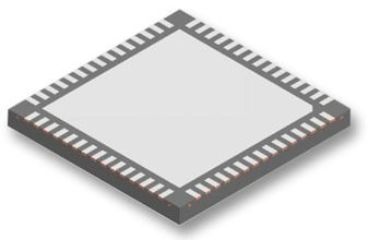
The ADC14DS080 is a high-performance CMOS analog-to-digital converter capable of converting two analog input signals into 14-bit digital words at rates up to 80 Mega Samples Per Second (MSPS). The digital outputs are serialized and provided on differential LVDS signal pairs. These converters use a differential, pipelined architecture with digital error correction and an on-chip sample-and-hold circuit to minimize power consumption and the external component count, while providing excellent dynamic performance. A unique sample-and-hold stage yields a full-power bandwidth of 1 GHz. The ADC14DS080 may be operated from a single +3.0V or 3.3V power supply. A power-down feature reduces the power consumption to very low levels while still allowing fast wake-up time to full operation. The differential inputs accept a 2V full scale differential input swing. A stable 1.2V internal voltage reference is provided, or the ADC14DS080 can be operated with an external 1.2V reference. Output data format (offset binary versus 2"s complement) and duty cycle stabilizer are selectable. The duty cycle stabilizer maintains performance over a wide range of clock duty cycles. A serial interface allows access to the control registers for full control of the ADC14DS80 functionality. The ADC14DS080 is available in a 60-lead WQFN package and operates over the industrial temperature range of -40°C to +85°C.