ADC Dual Pipelined 80Msps 12-bit Serial 60-Pin LLP EP T/R, ADC12DS080CISQ, Texas Instruments

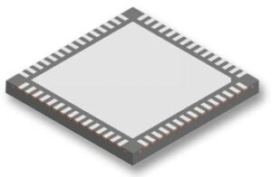
The ADC12DS080 is a high-performance CMOS analog-to-digital converter capable of converting two analog input signals into 12-bit digital words at rates up to 80 Mega Samples Per Second (MSPS). The digital outputs are serialized and provided on differential LVDS signal pairs. This converter uses a differential, pipelined architecture with digital error correction and an on-chip sample-and-hold circuit to minimize power consumption and the external component count, while providing excellent dynamic performance. The ADC12DS080 may be operated from a single +3.0V or 3.3V power supply. A power-down feature reduces the power consumption to very low levels while still allowing fast wake-up time to full operation. The differential inputs accept a 2V full scale differential input swing. A stable 1.2V internal voltage reference is provided, or the ADC12DS080 can be operated with an external 1.2V reference. The selectable duty cycle stabilizer maintains performance over a wide range of clock duty cycles. A serial interface allows access to the internal registers for full control of the ADC12DS080"s functionality. The ADC12DS080 is available in a 60-lead WQFN package and operates over the industrial temperature range of -40°C to +85°C 
  • Clock Duty Cycle Stabilizer
  • Single +3.0 or 3.3V Supply Operation
  • Serial LVDS Outputs
  • Serial Control Interface
  • Overrange Outputs
  • 60-pin WQFN Package, (9x9x0.8mm, 0.5mm pin-pitch)
  • High IF Sampling Receivers
  • Wireless Base Station Receivers
  • Test and Measurement Equipment
  • Communications Instrumentation
  • Portable Instrumentation
  • Характеристики

    Volt_supply_source

    Single

    Number_of_analog_inputs

    2

    Sampling_rate

    80 Msps

    Volt_reference

    External, Internal

    Digital_supply_support

    No

    Architecture

    Pipelined

    Resolution

    12 Bit

    Differential_nonlinearity

    0.5 LSB

    Signal_to_noise_ratio

    71 dBFS

    Input_type

    Voltage

    Input_signal_type

    Differential

    Input_volt

    2 Vp-p

    Бренд

    Msl_level

    3

    Country_of_origin

    United States

    Eccn

    EAR99

    Htsn

    8542390001

    Lead_finish

    Tin/Lead

    Max_power_dissipation

    845 mW

    Max_processing_temp

    260

    Mounting

    Surface Mount

    Operating_temp

    -40 to 85 °C

    Pin_count

    60

    Product_dimensions

    9 x 9 x 0.8 mm

    Schedule_b

    8542390000

    Screening_level

    Industrial

    Specifications

    http://www.ti.com/lit/ds/symlink/adc12ds080.pdf

    Supplier_package

    LLP EP

    Operating_supply_volt

    2.7, 3 V, 3.6

    Number_of_adcs

    2

    Digital_interface_type

    LVDS, Serial

    Артикул: ADC12DS080CISQ

    Описание

    The ADC12DS080 is a high-performance CMOS analog-to-digital converter capable of converting two analog input signals into 12-bit digital words at rates up to 80 Mega Samples Per Second (MSPS). The digital outputs are serialized and provided on differential LVDS signal pairs. This converter uses a differential, pipelined architecture with digital error correction and an on-chip sample-and-hold circuit to minimize power consumption and the external component count, while providing excellent dynamic performance. The ADC12DS080 may be operated from a single +3.0V or 3.3V power supply. A power-down feature reduces the power consumption to very low levels while still allowing fast wake-up time to full operation. The differential inputs accept a 2V full scale differential input swing. A stable 1.2V internal voltage reference is provided, or the ADC12DS080 can be operated with an external 1.2V reference. The selectable duty cycle stabilizer maintains performance over a wide range of clock duty cycles. A serial interface allows access to the internal registers for full control of the ADC12DS080"s functionality. The ADC12DS080 is available in a 60-lead WQFN package and operates over the industrial temperature range of -40°C to +85°C 
  • Clock Duty Cycle Stabilizer
  • Single +3.0 or 3.3V Supply Operation
  • Serial LVDS Outputs
  • Serial Control Interface
  • Overrange Outputs
  • 60-pin WQFN Package, (9x9x0.8mm, 0.5mm pin-pitch)
  • High IF Sampling Receivers
  • Wireless Base Station Receivers
  • Test and Measurement Equipment
  • Communications Instrumentation
  • Portable Instrumentation
  • Детали

    Volt_supply_source

    Single

    Number_of_analog_inputs

    2

    Sampling_rate

    80 Msps

    Volt_reference

    External, Internal

    Digital_supply_support

    No

    Architecture

    Pipelined

    Resolution

    12 Bit

    Differential_nonlinearity

    0.5 LSB

    Signal_to_noise_ratio

    71 dBFS

    Input_type

    Voltage

    Input_signal_type

    Differential

    Input_volt

    2 Vp-p

    Бренд

    Msl_level

    3

    Country_of_origin

    United States

    Eccn

    EAR99

    Htsn

    8542390001

    Lead_finish

    Tin/Lead

    Max_power_dissipation

    845 mW

    Max_processing_temp

    260

    Mounting

    Surface Mount

    Operating_temp

    -40 to 85 °C

    Pin_count

    60

    Product_dimensions

    9 x 9 x 0.8 mm

    Schedule_b

    8542390000

    Screening_level

    Industrial

    Specifications

    http://www.ti.com/lit/ds/symlink/adc12ds080.pdf

    Supplier_package

    LLP EP

    Operating_supply_volt

    2.7, 3 V, 3.6

    Number_of_adcs

    2

    Digital_interface_type

    LVDS, Serial