Описание
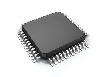
The ADC10D020 is a dual low power, high performance CMOS analog-to-digital converter that digitizes signals to 10 bits resolution at sampling rates up to 30 MSPS while consuming a typical 150 mW from a single 3.0V supply. No missing codes is ensured over the full operating temperature range. The unique two stage architecture achieves 9.5 Effective Bits over the entire Nyquist band at 20 MHz sample rate. An output formatting choice of offset binary or 2"s complement coding and a choice of two gain settings eases the interface to many systems. Also allowing great flexibility of use is a selectable 10-bit multiplexed or 20-bit parallel output mode. An offset correction feature minimizes the offset error.To ease interfacing to most low voltage systems, the digital output power pins of the ADC10D020 can be tied to a separate supply voltage of 1.5V to 3.6V, making the outputs compatible with other low voltage systems. When not converting, power consumption can be reduced by pulling the PD (Power Down) pin high, placing the converter into a low power state where it typically consumes less than 1 mW and from which recovery is less than 1 ms. Bringing the STBY (Standby) pin high places the converter into a standby mode where power consumption is about 27 mW and from which recovery is 800 ns.The ADC10D020"s speed, resolution and single supply operation makes it well suited for a variety of applications, including high speed portable applications.Operating over the industrial (-40° = TA = +85°C) temperature range, the ADC10D020 is available in a 48-pin TQFP package. An evaluation board is available to ease the design effort.