Описание
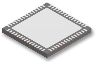
The ADC10DV200 is a monolithic analog-to-digital converter capable of converting two analog input signals into 10-bit digital words at rates up to 200 Mega Samples Per Second (MSPS). The digital output mode is selectable and can be either differential LVDS or CMOS signals. This converter uses a differential, pipelined architecture with digital error correction and an on-chip sample-and-hold circuit to minimize die size and power consumption while providing excellent dynamic performance. A unique sample-and-hold stage yields a full-power bandwidth of 900MHz. Fabricated in core CMOS process, the ADC10DV200 may be operated from a single 1.8V power supply. The ADC10DV200 achieves approximately 9.6 effective bits at Nyquist and consumes just 280mW at 170MSPS in CMOS mode and 450mW at 200MSPS in LVDS mode. The power consumption can be scaled down further by reducing sampling rates.