ADC Dual Pipelined 100Msps 8-bit Parallel 48-Pin TQFP EP, MAX1198ECM+D, Maxim Integrated

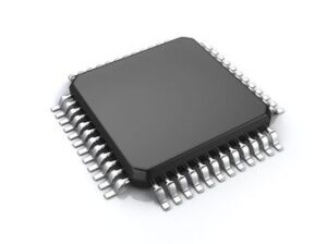
The MAX1198 is a 3.3V, dual, 8-bit analog-to-digital converter (ADC) featuring fully differential wideband track-and-hold (T/H) inputs, driving two ADCs. The MAX1198 is optimized for low power, small size, and high-dynamic performance for applications in imaging, instrumentation, and digital communications. This ADC operates from a single 2.7V to 3.6V supply, consuming only 264mW, while delivering a typical signal-to-noise and distortion (SINAD) of 48.1dB at an input frequency of 50MHz and a sampling rate of 100Msps. The T/H-driven input stages incorporate 400MHz (-3dB) input amplifiers. The converters may also be operated with single-ended inputs. In addition to low operating power, the MAX1198 features a 3.2mA sleep mode, as well as a 0.15µA power-down mode to conserve power during idle periods. An internal 2.048V precision bandgap reference sets the full-scale range of the ADC. A flexible reference structure allows the use of this internal or an externally applied reference, if desired, for applications requiring increased accuracy or a different input voltage range. The MAX1198 features parallel, CMOS-compatible three-state outputs. The digital output format can be set to two"s complement or straight offset binary through a single control pin. The device provides for a separate output power supply of 1.7V to 3.6V for flexible interfacing with various logic families. The MAX1198 is available in a 7mm x 7mm, 48-pin TQFP package, and is specified for the extended industrial (-40°C to +85°C) temperature range. See a parametric table of the complete family of pin-compatible, 8-bit high-speed ADCs. For a 10-bit, pin-compatible upgrade, refer to the MAX1180 data sheet. With the N.C. pins of the MAX1198 internally pulled down to ground, this ADC becomes a drop-in replacement for the MAX1180.

  • Single 2.7V to 3.6V Operation
  • Excellent Dynamic Performance
    • 48.1dB/47.6dB SINAD at fIN = 50MHz/200MHz
    • 66dBc/61.5dBc SFDR at fIN = 50MHz/200MHz
  • -72dB Interchannel Crosstalk at fIN = 50MHz
  • Low Power
    • 264mW (Normal Operation)
    • 10.6mW (Sleep Mode)
    • 0.5µW (Shutdown Mode)
  • 0.05dB Gain and ±0.1° Phase Matching
  • Wide ±1VP-P Differential Analog Input Voltage Range
  • 400MHz -3dB Input Bandwidth
  • On-Chip 2.048V Precision Bandgap Reference
  • User-Selectable Output Format-Two"s Complement or Offset Binary
  • Pin-Compatible 8-Bit and 10-Bit Upgrades Available
  • Характеристики

    Volt_supply_source

    Single

    Number_of_analog_inputs

    2

    Country_of_origin

    Korea, South

    Msl_level

    3

    Бренд

    Input_volt

    ±1 V

    Input_signal_type

    Differential, Single-Ended

    Input_type

    Voltage

    Differential_nonlinearity

    1 LSB

    Signal_to_noise_ratio

    48.5 dB

    Typical_power_dissipation

    264 mW

    Resolution

    8 Bit

    Architecture

    Pipelined

    Digital_supply_support

    No

    Volt_reference

    External, Internal

    Sampling_rate

    100 Msps

    Eccn

    EAR99

    Htsn

    8542390001

    Lead_finish

    Matte Tin

    Number_of_adcs

    2

    Operating_supply_volt

    2.7, 3.3 V, 3.6

    Polarity_of_input_volt

    Bipolar

    Number_of_adc_channels

    2

    Supplier_package

    TQFP EP

    Specifications

    https://4donline.ihs.com/images/VipMasterIC/IC/MAXM/MAXMS07920/MAXMS07920-1.pdf?hkey=52A5661711E402568146F3353EA87419

    Schedule_b

    8542390000

    Screening_level

    Extended Industrial

    Product_dimensions

    7 x 7 x 1 mm

    Pin_count

    48

    Operating_temp

    -40 to 85 °C

    Mounting

    Surface Mount

    Max_processing_temp

    260, 300

    Max_power_dissipation

    314 mW

    Digital_interface_type

    Parallel

    Артикул: MAX1198ECM+D

    Описание

    The MAX1198 is a 3.3V, dual, 8-bit analog-to-digital converter (ADC) featuring fully differential wideband track-and-hold (T/H) inputs, driving two ADCs. The MAX1198 is optimized for low power, small size, and high-dynamic performance for applications in imaging, instrumentation, and digital communications. This ADC operates from a single 2.7V to 3.6V supply, consuming only 264mW, while delivering a typical signal-to-noise and distortion (SINAD) of 48.1dB at an input frequency of 50MHz and a sampling rate of 100Msps. The T/H-driven input stages incorporate 400MHz (-3dB) input amplifiers. The converters may also be operated with single-ended inputs. In addition to low operating power, the MAX1198 features a 3.2mA sleep mode, as well as a 0.15µA power-down mode to conserve power during idle periods. An internal 2.048V precision bandgap reference sets the full-scale range of the ADC. A flexible reference structure allows the use of this internal or an externally applied reference, if desired, for applications requiring increased accuracy or a different input voltage range. The MAX1198 features parallel, CMOS-compatible three-state outputs. The digital output format can be set to two"s complement or straight offset binary through a single control pin. The device provides for a separate output power supply of 1.7V to 3.6V for flexible interfacing with various logic families. The MAX1198 is available in a 7mm x 7mm, 48-pin TQFP package, and is specified for the extended industrial (-40°C to +85°C) temperature range. See a parametric table of the complete family of pin-compatible, 8-bit high-speed ADCs. For a 10-bit, pin-compatible upgrade, refer to the MAX1180 data sheet. With the N.C. pins of the MAX1198 internally pulled down to ground, this ADC becomes a drop-in replacement for the MAX1180.

    • Single 2.7V to 3.6V Operation
    • Excellent Dynamic Performance
      • 48.1dB/47.6dB SINAD at fIN = 50MHz/200MHz
      • 66dBc/61.5dBc SFDR at fIN = 50MHz/200MHz
  • -72dB Interchannel Crosstalk at fIN = 50MHz
  • Low Power
    • 264mW (Normal Operation)
    • 10.6mW (Sleep Mode)
    • 0.5µW (Shutdown Mode)
  • 0.05dB Gain and ±0.1° Phase Matching
  • Wide ±1VP-P Differential Analog Input Voltage Range
  • 400MHz -3dB Input Bandwidth
  • On-Chip 2.048V Precision Bandgap Reference
  • User-Selectable Output Format-Two"s Complement or Offset Binary
  • Pin-Compatible 8-Bit and 10-Bit Upgrades Available
  • Детали

    Volt_supply_source

    Single

    Number_of_analog_inputs

    2

    Country_of_origin

    Korea, South

    Msl_level

    3

    Бренд

    Input_volt

    ±1 V

    Input_signal_type

    Differential, Single-Ended

    Input_type

    Voltage

    Differential_nonlinearity

    1 LSB

    Signal_to_noise_ratio

    48.5 dB

    Typical_power_dissipation

    264 mW

    Resolution

    8 Bit

    Architecture

    Pipelined

    Digital_supply_support

    No

    Volt_reference

    External, Internal

    Sampling_rate

    100 Msps

    Eccn

    EAR99

    Htsn

    8542390001

    Lead_finish

    Matte Tin

    Number_of_adcs

    2

    Operating_supply_volt

    2.7, 3.3 V, 3.6

    Polarity_of_input_volt

    Bipolar

    Number_of_adc_channels

    2

    Supplier_package

    TQFP EP

    Specifications

    https://4donline.ihs.com/images/VipMasterIC/IC/MAXM/MAXMS07920/MAXMS07920-1.pdf?hkey=52A5661711E402568146F3353EA87419

    Schedule_b

    8542390000

    Screening_level

    Extended Industrial

    Product_dimensions

    7 x 7 x 1 mm

    Pin_count

    48

    Operating_temp

    -40 to 85 °C

    Mounting

    Surface Mount

    Max_processing_temp

    260, 300

    Max_power_dissipation

    314 mW

    Digital_interface_type

    Parallel